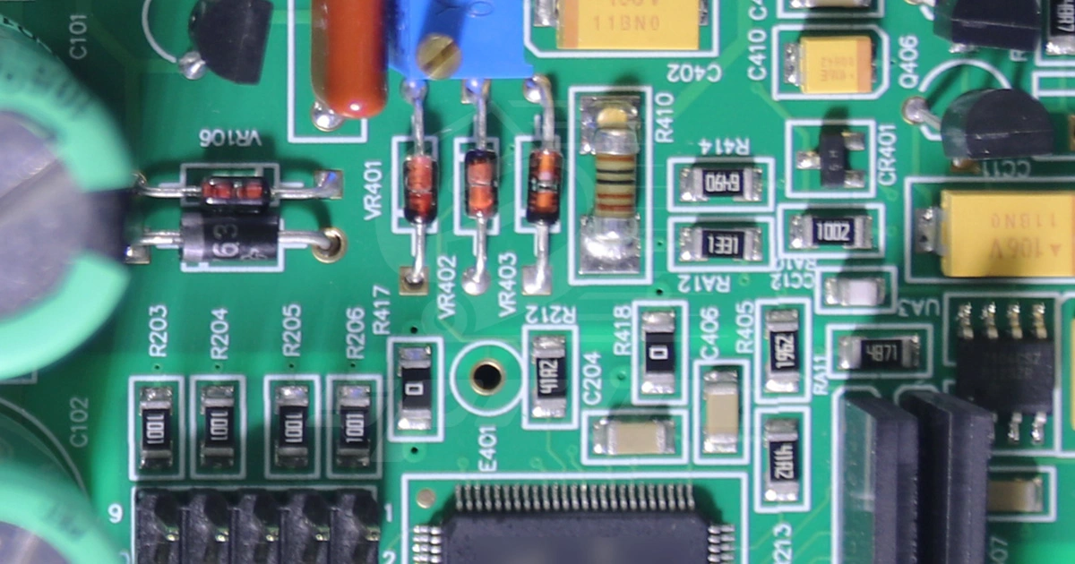
In high-speed Printed Circuit Board (PCB) design, Via Plugging plays a crucial role. With the increasing complexity and speed of electronic devices, the application of Via Plugging technology has become increasingly important. It not only enhances the performance and reliability of the circuit board but also effectively reduces signal interference and transmission loss. This article comprehensively introduces the definition, function, implementation and application, standard sizes, and commonly used Via Plugging techniques to help readers better understand and apply this key technology.
Now, let's delve into commonly used Via Plugging techniques. In high-speed PCB design, there are several commonly used Via Plugging techniques to choose from, including resistor filling, dielectric layer filling, and resin filling. Each technique has its unique advantages and applicable scenarios. Resistor filling can provide damping to signals, reducing reflections and interference. Dielectric layer filling can provide electromagnetic shielding and mechanical support. Resin filling can offer improved signal integrity and thermal conductivity. Choosing the appropriate Via Plugging technique that suits specific application requirements is crucial. First, let us introduce three types of resin filling techniques.
Electroplugging: This method utilizes the electroplating process to fill through-holes. Firstly, a thin layer of conductive material, such as copper, is coated on the through-hole. Then, electroplating is carried out. During the electroplating process, copper gradually deposits inside the through-hole, filling the aperture until the through-hole is completely plugged. This method provides reliable filling results and exhibits good conductivity.
Conductive Adhesive Plugging: This method utilizes conductive adhesive to fill through-holes. Conductive adhesive is typically composed of conductive particles, such as silver or carbon nanomaterials, and a binder. In this method, the conductive adhesive is injected into the through-hole, filling the aperture, and creating a conductive pathway with the conductive traces. Once the conductive adhesive cures, it provides excellent conductivity and mechanical support.
Copper Capping: This method involves adding a layer of copper above a via hole. First, a conductive adhesive is applied on top of the via hole, and then a copper foil or copper sheet is placed over it. Through heating and pressure treatment, the copper capping layer tightly bonds to the surface of the circuit board, filling and sealing the via hole. Copper capping provides good conductivity and strong mechanical support.
When it comes to resin filling technology, here are some common methods and steps:
Methods
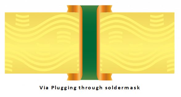
Via Tenting: This involves filling the through-holes with resin and forming a resin mask on the surface of the PCB to isolate the through-holes and provide protection. Via Filling: In this method, resin is injected into the through-holes to completely fill them and ensure that the resin is level with the PCB surface.
Micro-via Filling: This technique uses resin filling in micro-vias, which is typically applicable to high-density interconnect PCB designs.
Steps:
Preparation: Before performing resin filling technology, it is necessary to ensure that the PCB surface is clean and free of dust and prepare the tools and materials suitable for resin filling.
Coating solder mask layer (optional): Before resin filling, a layer of solder mask can be applied to the PCB surface to prevent resin from penetrating into areas where filling is not required.
Resin injection: Using appropriate resin injection tools or techniques, inject resin into the through-holes, ensuring that the through-holes are completely filled and reach the desired filling level.
Bubble elimination: During the resin filling process, bubbles may be generated, and measures need to be taken to eliminate them and ensure the integrity of the resin filling.
Removal of excess resin: After the resin has fully cured, it is necessary to remove the excess resin, making the filled through-holes flush with the PCB surface.
Features:
Signal Integrity: The use of encapsulation resin can provide excellent signal integrity by reducing signal loss and interference.
Mechanical Support: Encapsulation resin can provide additional mechanical support for through-holes, enhancing the structural strength of the PCB.
Thermal Conductivity: Certain encapsulation resins exhibit good thermal conductivity, which can aid in heat dissipation and cooling in high-power applications.
Environmental Protection: Encapsulation resin prevents moisture and impurities from entering through-holes, thereby improving the environmental protection performance of the PCB.
Secondly, there is the method of dielectric layer filling. Here are some common dielectric layer filling methods:
Glass Fiber Prepreg: Glass fiber prepreg, which is a layer of glass fiber impregnated with resin, is used as the dielectric material, and is filled into the through-holes through processes such as thermal pressing or curing. This method provides good mechanical support and stability, and effectively reduces electromagnetic interference during signal transmission.
Polymer Film: Polymer films, such as polyimide, are used as the dielectric layer to fill the through-holes. These films exhibit excellent insulation performance and high-temperature stability, providing effective electromagnetic shielding and reducing crosstalk and losses in high-speed signal transmission.
Resin Filling: Resin filling refers to the process of filling through-holes with specific filling resins, such as epoxy resin. The filling resin possesses excellent insulation and thermal conductivity properties, providing a stable signal transmission path and assisting in heat dissipation. This method typically involves filling the through-holes with the filling resin through vacuum or pressure injection.
Electrolyte Filling: Electrolyte filling involves the use of electrolyte, typically a liquid that conducts ions, to fill through-holes and create an electrolyte layer. This method is commonly applied in special high-frequency or high-speed applications, where the presence of the electrolyte layer enables lower transmission losses and better signal integrity. Here is a bullet-pointed explanation of the steps and characteristics of dielectric layer filling:
Steps:
Preparing vias: Firstly, identify the positions and quantity of vias that require dielectric layer filling in the PCB design. Then, create vias on the circuit board using drilling or laser techniques.
Cleaning and Preprocessing: Prior to filling the dielectric layer, it is necessary to thoroughly clean the through-holes and the surrounding area to remove any impurities or residues. Next, necessary preprocessing steps, such as surface treatment or oxidation removal, are carried out to ensure good adhesion of the dielectric layer.
Dielectric Material Filling: Select an appropriate dielectric material, such as epoxy resin or polyimide, and inject it into the through-holes according to design requirements and specific application needs. Dielectric material filling can be done using injection techniques, vacuum sealing, or coating methods.
Removal of Excess Material: Once the dielectric material is filled into the through-holes, excess material needs to be removed. Mechanical cutting, grinding, or chemical etching methods can be employed to level the surface of the circuit board and eliminate excess dielectric material.
Features:
Electromagnetic Shielding: By filling the dielectric material, a continuous dielectric layer is formed around the via, which can effectively shield electromagnetic radiation and interference signals, and improve the circuit's anti-interference performance.
Mechanical Support: The filled dielectric material can provide additional mechanical support, enhance the mechanical strength and reliability of the via, and reduce damage or fracture caused by physical stress.
Thermal Conductivity: Certain dielectric materials have good thermal conductivity, which can help effectively dissipate the heat generated around the via and improve the heat dissipation performance of the circuit board.
Finally, resistor filling technology is a commonly used Via Plugging technique aimed at damping and controlling signals by filling the through-holes with a material that possesses resistive properties. Here are several common resistor filling methods:
Silicon carbide filling: This method involves filling the through-holes with silicon carbide material. Silicon carbide exhibits good conductivity and thermal conductivity, enabling it to provide a certain level of resistance. This method is commonly employed for damping high-speed signals and controlling interference.
Carbon ink filling: Fill through-holes with conductive carbon ink or conductive adhesive. Carbon ink has high conductivity and can effectively achieve signal damping and suppress reflections.
Resistive filling coating: Cover through-holes with specialized resistive filling coatings. These coatings are typically composed of conductive particles and base resins, and the resistance value is controlled by adjusting the concentration of the coating. Resistor filling technology is a common Via Plugging technique used to achieve specific resistance values by filling the through-holes with resistor material. Here are the steps and features of resistor filling technology:
Steps:
Through-hole preparation: Firstly, determine the locations and quantity of through-holes that require resistor filling in the PCB design. These through-holes are typically located next to high-speed signal lines to provide damping and suppress reflections.
Material selection: Choose a suitable resistor filling material, typically an adhesive or conductive filler material with resistance characteristics. These materials should have good adhesion, conductivity, and thermal stability.
Filling the through-holes: Use appropriate methods and tools to inject the resistor filling material into the through-holes. Filling can be done manually or automatically, ensuring that the through-holes are fully filled, and the resistor material is evenly distributed.
Material curing: After filling the through-holes, the resistor filling material needs to be cured or hardened. This can be achieved through methods such as heat curing or UV curing.
Features:
Resistance control: Resistance filling technology allows precise control of the resistance value in the via, according to design requirements, to meet specific circuit demands.
Reflection suppression: By filling the via adjacent to the signal path with resistive material, signal reflections can be effectively suppressed, improving signal integrity and stability.
Signal damping: Resistance filling introduces damping effects alongside the signal line, reducing rise time and amplitude, and minimizing oscillations and interference at signal edges.
Space-saving: Compared to other Via Plugging techniques, resistance filling technology does not require additional dielectric layers or filling materials, allowing better utilization of PCB space.
These methods can provide resistance effects to a certain extent during the process of via plugging, reducing signal reflection and interference. The specific choice of resistor filling method depends on factors such as design requirements, signal frequency, and performance requirements. These are common Via Plugging techniques, and each technique has its own applicable scenarios and characteristics. In practical applications, it is crucial to select the appropriate Via Plugging technique based on specific design requirements and cost-effectiveness. Through a comprehensive overview in this article, we have gained a deeper understanding of the importance of Via Plugging in high-speed PCBs. By filling the through-holes, we can enhance the performance and reliability of the circuit board while reducing signal interference and transmission loss. Implementing Via Plugging technology requires adhering to standard via sizes and selecting appropriate Via Plugging techniques. In the ever-evolving realm of electronic devices and high-speed communication, Via Plugging will continue to play a crucial role in helping us build more reliable and efficient electronic systems.

Customer support