The utilization of a high-quality solder mask is crucial in the manufacturing process of printed circuit boards. If a PCB lacks a reliable solder mask, its durability will be significantly reduced. Creating an effective solder mask involves several factors and is a critical component of your PCB's composition.
What is a Solder Mask?
Solder mask is a liquid photoimageable lacquer used to safeguard the copper on the circuit board by providing a protective layer. It is applied to both sides of the PCB to shield the copper from various issues that could cause malfunction, such as oxidation, external conductive influences, soldering, high voltage spikes, environmental elements, and others.
During the printed circuit board fabrication process, the solder mask is sprayed onto the production panel, and then UV exposure is applied with the appropriate solder mask pattern. Subsequently, the mask is developed and dried. Although green is a common color for solder mask on PCBs, it is also available in other colors, and clear solder mask is also an option.
Importance of Solder Mask
The solder mask serves multiple purposes in the manufacturing process and overall functionality of printed circuit boards (PCBs). Apart from protecting the copper traces from various factors as mentioned before, it also prevents solder bridging between adjacent pads during assembly, enhances the visual contrast for easier inspection, and helps with component placement accuracy.
Types of Solder Mask
While green is the most common color for a solder mask on PCBs, there are various other color options available, such as red, blue, black, white, and more. The choice of color can be based on aesthetics, branding requirements, or specific applications. Additionally, a clear solder mask is also an option, which provides transparency for applications where visibility of underlying features is necessary.
Solder Mask Application Methods
There are different methods for applying solder mask to the PCB surface. The most used methods include screen printing, liquid photoimageable solder mask (LPI), and dry film solder mask. Each method has its advantages and is chosen based on factors like production volume, complexity of the design, and cost considerations.
Solder Mask Testing and Inspection
To ensure the quality and reliability of the solder mask, various testing and inspection methods are employed. One such method is the measurement of solder mask thickness, as mentioned earlier. Other tests include solder mask adhesion testing, chemical resistance testing, thermal cycling, and electrical testing to ensure the mask's effectiveness in different conditions.
Advances in Solder Mask Technology
Solder mask technology continues to evolve, driven by the demand for higher-density PCBs, miniaturization, and increased functionality. Manufacturers are developing advanced solder mask materials that offer improved thermal resistance, better adhesion to various substrate materials, enhanced electrical insulation properties, and compatibility with newer assembly techniques like advanced packaging technologies.
Environmental Considerations
In recent years, there has been a growing focus on environmental sustainability in the PCB manufacturing industry. Many companies are adopting eco-friendly solder mask materials that comply with RoHS (Restriction of Hazardous Substances) and REACH (Registration, Evaluation, Authorization, and Restriction of Chemicals) regulations, reducing the use of harmful substances and minimizing the impact on the environment.
How to Measure Solder Mask Thickness?
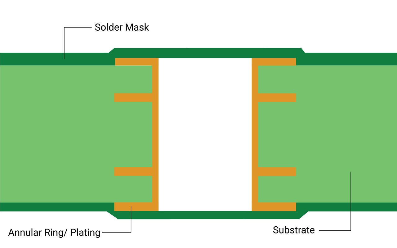
While a sufficient thickness of solder mask is necessary to safeguard the circuits, it's crucial to measure the solder mask's thickness to ensure it's not excessive. For the conductor's top and side edges, a thickness greater than 7 microns is preferred. The maximum thickness for solder masks on finished copper parts up to 35 micrometers is 40 micrometers, while for thicker copper, it can be up to 80 micrometers.
To ensure the effectiveness of the solder mask, it's recommended to follow the following guidelines:
- Meet the minimum annular ring requirements if the solder resist comes into contact with the lands.
- Avoid leaving exposed isolated pads.
- Allow solder resist only on plated through holes that are not intended for solder fill.
- Avoid applying solder resist on test points or connector fingers.
Achieving the appropriate thickness when applying solder mask is a delicate process and is one of many challenges that manufacturers face when producing high-quality printed circuit boards. At Sprintpcb, we have extensive experience in all aspects of well-designed PCB manufacturing, and we are delighted to share our knowledge with you.
If you require more information on solder mask thickness requirements, methods for measuring solder mask thickness, or any other issues relating to the manufacturing, distribution, or quality assessment of printed circuit boards, we are here to assist you. Contact Sprintpcb today to speak with one of our skilled PCB professionals.