The Overview of Copper Foil:
The development of electrolytic copper foil can be divided into three stages:
The establishment of American copper foil enterprises marked the beginning of the global electrolytic copper foil industry (1955 to the mid-1970s).
The rapid development of Japanese copper foil enterprises led to comprehensive dominance of the world market (1974 to the early 1990s).
The stage of diversification and competition among copper foil enterprises from Japan, the United States, Asia, and other regions (since the mid-1990s to the present). Japan is the world's largest producer of copper foil, followed by Taiwan, China.
The copper foil industry originated from the copper smelter of Anaconda Company in New Jersey, USA, in 1937. In 1955, Yates Corporation in the United States began specialized production of copper foil for PCBs.
China started producing copper foil in the early 1960s and has now formed a relatively complete industrial chain.
The StandardsforCopper Foil:
There are several main standards for Copper Foil:
American ANSI/IPC Standards: IPC-CF-150 (1966), IPC-MF-150G (1999), IPC-4562 (currently in use).
European IEC Standards: IEC-249-3A (1976).
Japanese JIS Standards: JIS-C-6511 (1992), JIS-C-6512 (1992), JIS-C-6513 (1996).
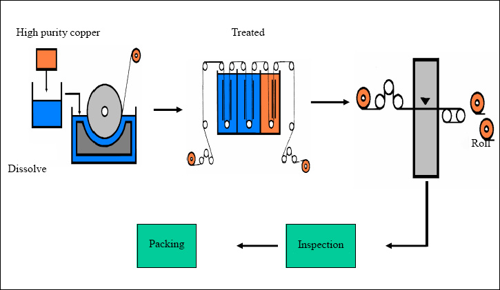
The Production Process Diagramfor Copper Foil:
Thetypes and Roughness of Commonly Used PCB Copper Foils:
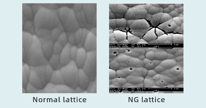
The crystal Phase Structure of the Electrolytic Copper Foil Surface:
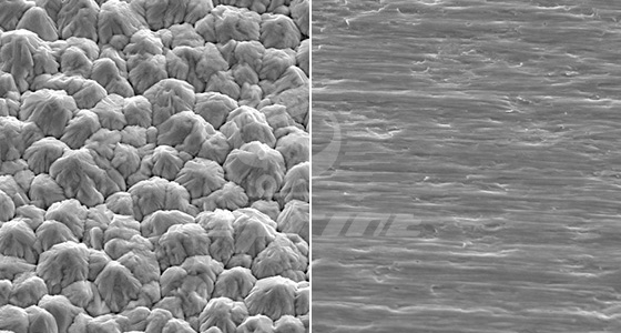
The Matte Surface for Copper Foil Copper Foil Shiny Surface
- STD: Standard Electrolytic Copper Foil
- HTE: High-Temperature High-Ductility Copper Foil, commonly used by PCB manufacturers
- RTF: The double-sided treatment copper foil, also called reverse copper foil, means that the smooth side is also roughened.
- UTF: Ultra-Thin copper Foil, whosethinner than 9μm.
- RCC: Resin Coated Copper Foil, whichwastypically used for HDI board lamination.
- LP: Low Profile Copper Foil, whichwaswith roughened matte surface for high-speed boards.
- VLP: UltraLow Profile Copper Foil.
- HVLP: High-Frequency UltraLow Profile Copper Foil, whichwas used for high-frequency high-speed boards.
The roughness of standard copper foil (STD) is approximately 7-8μm, while for reverse treated copper foil (VLP), it is around 4-6μm. Low roughness copper foil has a roughness of approximately 3-4μm, and ultra-low roughness copper foil has a roughness of around 1.5-2μm.
IPC-4562 specifies the types and codes of metal foils based on their manufacturing processes:
- E: Electrodeposited Foil
- W: Wrought Foil
- O: Other Foils
Introduction to Copper Foil Types
Copper Foil:
Refers to pure copper foil, used in printed circuits for the metallic copper layer on pressed copper-clad laminates or outer layers of multilayer boards.
Electrodeposited Copper Foil (ED Copper Foil):
Refers to copper foil made by electrodeposition. The manufacture of electrolytic copper foil for printed circuit boards begins with the production of original foil (also known as "raw foil" ). Its manufacturing process is an electrolytic process. Electrolysis equipment generally uses a surface roller made of titanium material as the cathode roller, and uses high-quality soluble lead-based alloy or insoluble titanium-based corrosion-resistant coating (DSA) as the anode. Copper sulfate electrolyte is added between the cathode and anode. Under the action of direct current, metal copper ions are adsorbed on the cathode roller to form electrolytic original foil. As the cathode roller continues to rotate, the generated original foil
Rolled Copper Foil:
The Copper foil produced by rolling method, which is also known as wrought copper foil.
The double-sided treatment copper foil:
It means that in addition to processing the rough surface of the electrolytic copper foil, the smooth surface is also processed to make it rough. Using this copper foil as the inner layer of the multi-layer board does not need to be roughened before laminating the multi-layer board (black chemical) processing.
High-Temperature Elongation Copper Foil (HTE Copper Foil):
The copper foil with excellent elongation at high temperatures (180°C). For 35μm and 70μm thickness copper foils, the elongation at high temperature (180°C) should be maintained at more than 30% of the elongation at room temperature. It’s also known as HD copper foil (high ductility copper foil).
Low Profile Copper Foil (LP):
The microcrystallization of the original foil of the general copper foil is very rough, with coarse columnar crystals. The prisms of the transverse faults of its slices, undulate a lot. The crystallization of low-profile copper foil is very fine (below 2 μm), isometric grains, does not contain columnar crystals, is lamellar crystallization in slices, and the prisms are flat. The roughness of the surface is low. Ultra-low profile electrolytic copper foil is actually measured, and the average roughness (Ra) is 0.55 μm (general copper foil is 1.40 μm). The maximum roughness is 5.04μm (12.50μm for general copper foil).
Resin Coated Copper Foil (RCC):
It’s known as resin-attached copper foil in China, is called adhesive-backed copper foil in Taiwan, and called the insulating resin sheet which loaded on the copper foil, or a adhesive film with copper foil internationally .It is made of thin electrolytic copper foil (thickness generally ≤ 18) μ m) The rough surface is coated with one or two layers of specially composed resin adhesive (the main component of the resin is usually epoxy resin), which is processed and dried in an oven to remove solvents and resin, forming a semi cured B-stage form. The thickness used for RCC generally does not exceed 18 μ m. Currently commonly used 12 μ Mainly m, the thickness of the resin layer is generally between 40-100 μ M. It plays a role in replacing the traditional semi cured sheet and copper foil in the production process of laminated multilayer boards. As an insulation medium and conductor layer, it can be pressed together with the core board using a similar process as traditional multi-layer board pressing to manufacture laminated multilayer boards.
Ultra-Thin Copper Foil:
It’s refer to copper foil with a thickness below 9μm used in printed circuit boards. Typical copper foils have thicknesses above 12μm for outer layers of multilayer boards and above 18μm for inner layers. Copper foils thinner than 9μm are used in the manufacture of printed circuit boards with fine circuits. Due to the difficulty in handling ultra-thin copper foils, they are generally supported by carriers such as copper foil, aluminum foil, or organic thin films.The types of carriers include copper foil, aluminum foil, organic film, etc.