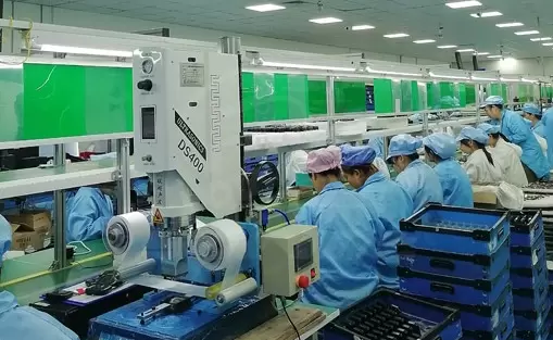
In the realm of electronics manufacturing, Multilayer PCBs (Printed Circuit Boards) have emerged as pivotal components facilitating intricate circuitry in various devices. SprintPCB, a distinguished Multilayer PCB manufacturer, orchestrates a meticulous manufacturing process to ensure the production of high-quality boards meeting diverse industry demands. There are 10 steps in the
multilayer PCB manufacturing process.
Multilayer PCB Design:
Multilayer PCB manufacturing process Step 1 is multilayer PCB design. Multilayer PCB fabrication commences with meticulous design. Engineers meticulously plan circuit layout, considering factors like signal integrity, power distribution, and thermal management. Advanced software aids in creating intricate designs tailored to specific applications. Through close collaboration with clients, SprintPCB's design team ensures that each board meets exact specifications, optimizing performance and functionality.
Multilayer PCB Inner Layer Production:
Multilayer PCB manufacturing process Step 2 is multilayer PCB inner layer production. Inner layer production involves laminating copper foil onto substrate layers. Automated equipment ensures precise alignment and adherence, crucial for maintaining signal integrity and minimizing impedance issues. SprintPCB utilizes state-of-the-art lamination techniques, employing controlled pressure and temperature profiles to achieve uniform copper distribution across the inner layers.
Multilayer PCB Drilling:
Multilayer PCB manufacturing process Step 3 is multilayer PCB drilling. Precision drilling is pivotal for creating vias that establish electrical connections between layers. Automated drilling machines with high-speed spindles ensure accuracy, while computerized control guarantees consistency across the board. SprintPCB's drilling process employs advanced drill bits and precise tooling to achieve microvia drilling, enabling the integration of complex designs into compact form factors.
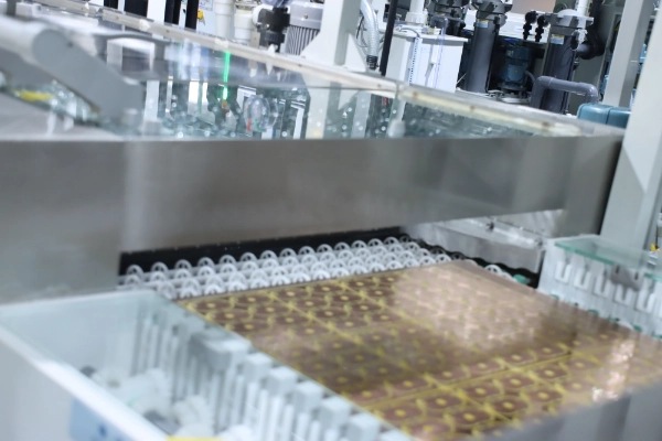
Multilayer PCB Chemical Copper Plating (Through-Hole Plating):
Multilayer PCB manufacturing process Step 4 is multilayer PCB chemical Copper Plating. Through-hole plating involves depositing a thin layer of copper onto drilled holes, ensuring conductivity between layers. Chemical baths facilitate the copper deposition process, with controlled parameters optimizing plating uniformity. SprintPCB meticulously monitors plating parameters, such as solution concentration and temperature, to achieve uniform copper deposition and reliable interlayer connections.
Multilayer PCB Stacking:
Multilayer PCB manufacturing process Step 5 is multilayer PCB stacking. Stacking involves sandwiching inner layers with prepreg layers, forming the Multilayer PCB stack. Automated equipment precisely aligns and compresses the stack, preparing it for lamination. SprintPCB's stacking process incorporates automated optical alignment systems, ensuring precise registration of layers and minimizing potential defects during subsequent processing stages.
Multilayer PCB Lamination:
Multilayer PCB manufacturing process Step 6 is multilayer PCB lamination. Lamination involves subjecting the stacked layers to heat and pressure, bonding them into a unified structure. This process ensures optimal electrical performance and mechanical stability while maintaining dimensional accuracy. SprintPCB utilizes advanced vacuum lamination techniques, eliminating voids and ensuring uniform resin distribution for enhanced reliability and durability.
Multilayer PCB Patterning (Photoengraving):
Multilayer PCB manufacturing process Step 7 is multilayer PCB patterning. Photoengraving employs photolithography techniques to transfer the circuit pattern onto the PCB surface. UV light exposure through a photoresist mask selectively etches away unwanted copper, delineating the circuit traces. SprintPCB's precision photolithography equipment and high-resolution imaging systems enable the fabrication of intricate circuit patterns with sub-micron accuracy, meeting the most demanding design requirements.
Multilayer PCB Chemical Copper Plating (Surface Plating):
Multilayer PCB manufacturing process Step 8 is multilayer PCB chemical copper plating. Surface plating deposits a thicker layer of copper onto the exposed circuit traces, enhancing conductivity and ensuring robust solderability. Chemical baths control plating thickness, promoting uniform coverage across the PCB surface. SprintPCB employs advanced electroplating techniques, coupled with rigorous quality control measures, to achieve precise copper thickness and uniformity, facilitating reliable soldering and assembly processes.
Multilayer PCB Curing:
Multilayer PCB manufacturing process Step 9 is multilayer PCB curing. Curing involves subjecting the PCB to controlled heat to cure the solder mask and ensure adhesion of surface finishes. Precise temperature and duration parameters prevent warping or delamination, preserving PCB integrity. SprintPCB's curing process is meticulously optimized to achieve uniform curing across the entire PCB surface, enhancing mechanical strength and reliability while maintaining dimensional stability.
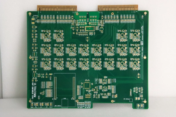
Multilayer PCB Final Processing:
Multilayer PCB manufacturing process Step 10 is multilayer PCB final processing. Final processing encompasses various post-production tasks, including routing, electrical testing, and quality inspection. Automated optical inspection (AOI) and electrical testing verify adherence to design specifications and identify any defects before shipment. SprintPCB's comprehensive final processing protocols ensure that each Multilayer PCB undergoes rigorous testing and inspection, guaranteeing compliance with industry standards and customer requirements.
In conclusion, SprintPCB's commitment to excellence is evident throughout the Multilayer PCB manufacturing process. From meticulous design to stringent quality control measures, each step contributes to the production of reliable and high-performance PCBs. As a leading Multilayer PCB supplier,
SprintPCB continues to drive innovation and meet the evolving needs of industries worldwide.