HDI PCB stands for High-Density Interconnect PCB, which is a type of technology used in the production of printed circuit boards. HDI PCBs are known for their high circuitry density and utilize micro-blind via technology. They represent one of the fastest-growing segments in the printed circuit board market. Due to the increased circuit density of HDI PCBs, it allows for the consolidation of finer lines and spaces, smaller through-holes, and capture pads, as well as a higher density of interconnection pads. HDI PCBs feature blind vias and buried vias and typically include micro-vias with diameters of 0.006 or smaller.
In September 1994, a cooperative consortium of the PCB industry in the United States, known as ITRI (Interconnection Technology Research Institute), embarked on research to produce high-density circuit boards, referred to as the October Project. They utilized Motorola's prototype MTV1 and MRTV2.2 (June 1996) to experiment with the production of micro blind vias using non-mechanical drilling methods. These methods included laser ablation, photo-via, plasma etching, and alkaline etching.The new era of High-Density Interconnect (HDI) circuit boards officially began with the publication of the October Project Phase I Round 2 Report on July 15, 1997. Initially, these products were referred to as SBU (Small Business Unit) in the Western countries, while in Japan, they were called MVP (Miniature Vias and Pads), due to their significantly smaller hole structures compared to previous boards. However, eventually, the American IPC (Association Connecting Electronics Industries) unified the terminology and named them "HDI."
The main difference between HDI PCB and traditional PCB
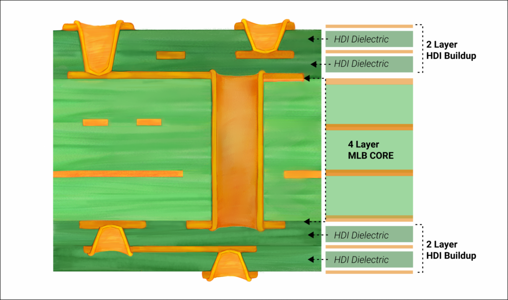
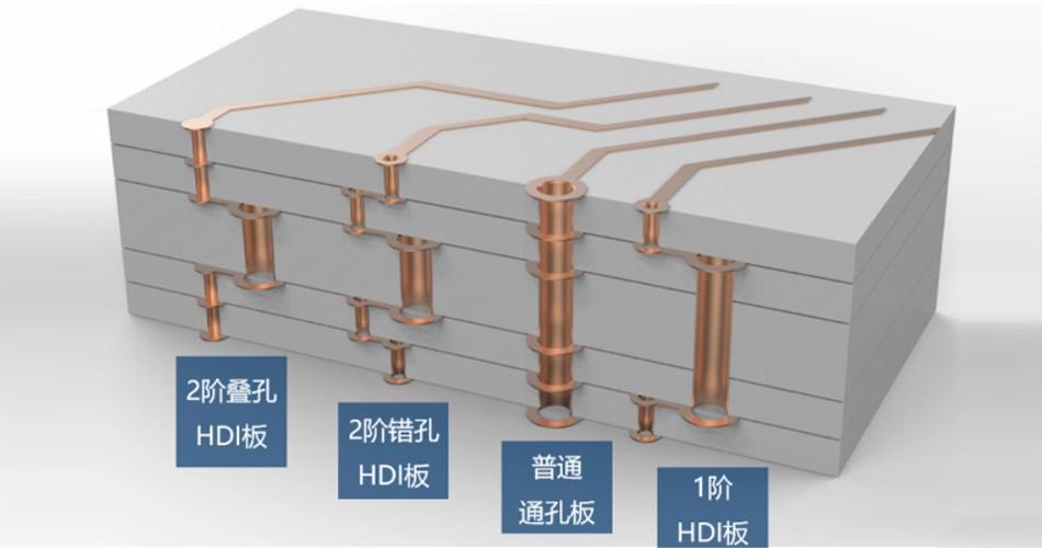
HDI boards, also known as Build-up Multilayer (BUM) boards, are constructed using traditional double-sided boards as the core substrate, which are continuously stacked and laminated. In comparison to conventional circuit boards, HDI boards offer advantages such as being lightweight, thin, short, and small. The electrical interconnections between layers in HDI boards are achieved through conductive vias, buried vias, and blind vias. The structural composition of HDI boards differs from regular multilayer boards as they extensively incorporate micro-buried blind vias.
Traditional multilayer circuit boards only have through-holes and do not have small buried blind vias. The electrical interconnections in these circuit boards are achieved through-hole connections, requiring a higher number of layers to meet design requirements. In contrast, HDI boards employ a micro buried blind via design, requiring fewer layers to meet design needs, making them lighter and thinner.
High reliability of HDI PCB
Copper pillars enhance reliability by reducing impedance mismatches between different metals used in the stack-up, due to their differing coefficients of thermal expansion. Furthermore, HDI boards exhibit lower sensitivity to environmental factors such as humidity and temperature compared to traditional printed circuit boards, thanks to their higher mechanical strength.
High-density interconnection of HDI PCB
The use of copper pillars enables high-density interconnection without increasing the number of layers on the circuit board. This provides greater flexibility in routing signals from one side of the board to the other without the need for expensive plated through-holes or blind vias. The presence of copper pillars also helps reduce crosstalk between signals routed on different layers by providing additional electrical connection points at each layer interface.
Smaller dimensions of HDI PCB
High-density interconnection is achieved by placing components closer together than traditional circuit boards, reducing the overall size of the circuit board while maintaining the same level of performance. For instance, medical devices often require small packaging with high transmission rates, which can only be provided by HDI PCBs. For example, implants need to be small enough to fit inside the human body, but any electronic devices involved in the implants must effectively allow high-speed signal transmission.
Reducing weight
The overall reduction in volume allows for thinner circuit boards without compromising performance or reliability. This also decreases the number of materials used during the production process, thereby lowering material costs and waste disposal expenses.
Lower Capacitance and Inductance of HDI PCB
Interconnects have lower capacitance and inductance compared to traditional PCBs, which helps improve signal integrity, reduce noise, and increase bandwidth.
Higher Performance of HDI PCB
HDI boards offer better heat dissipation and signal integrity compared to traditional PCBs. The higher density allows for smaller components and thinner layers while maintaining the required impedance characteristics. This results in superior performance in both digital and analog circuits, especially in terms of noise immunity and signal integrity.
Highly customizable
HDI PCBs offer a high degree of customization, allowing for not only the size and thickness of the circuit but also the ability to shape it according to specific requirements. This enables the construction of more intricate designs within smaller form factors, which is especially advantageous for space-constrained wireless devices like smartphones and tablets.
Lower cost of HDI PCB
HDI PCBs are more cost-effective to produce compared to traditional circuit boards. They require fewer copper layers per square inch, resulting in reduced production costs. Moreover, since they do not necessitate expensive through-hole components, their manufacturing expenses are lower than those of conventional circuit boards.
Type and number of through-holes or microholes: The type and quantity of vias or microvias in HDI PCBs will impact their cost. The cost is higher for smaller diameters compared to larger ones, as they require higher precision. Additionally, increasing the number of holes will also raise the price.
Stack height and layer count: The type of stack you require will also impact the cost. A 2-n-2 high-density PCB layout is more complex than a 1-n-1, therefore it will be more expensive. Additional layers will increase the price. You need to choose the most cost-effective layer count.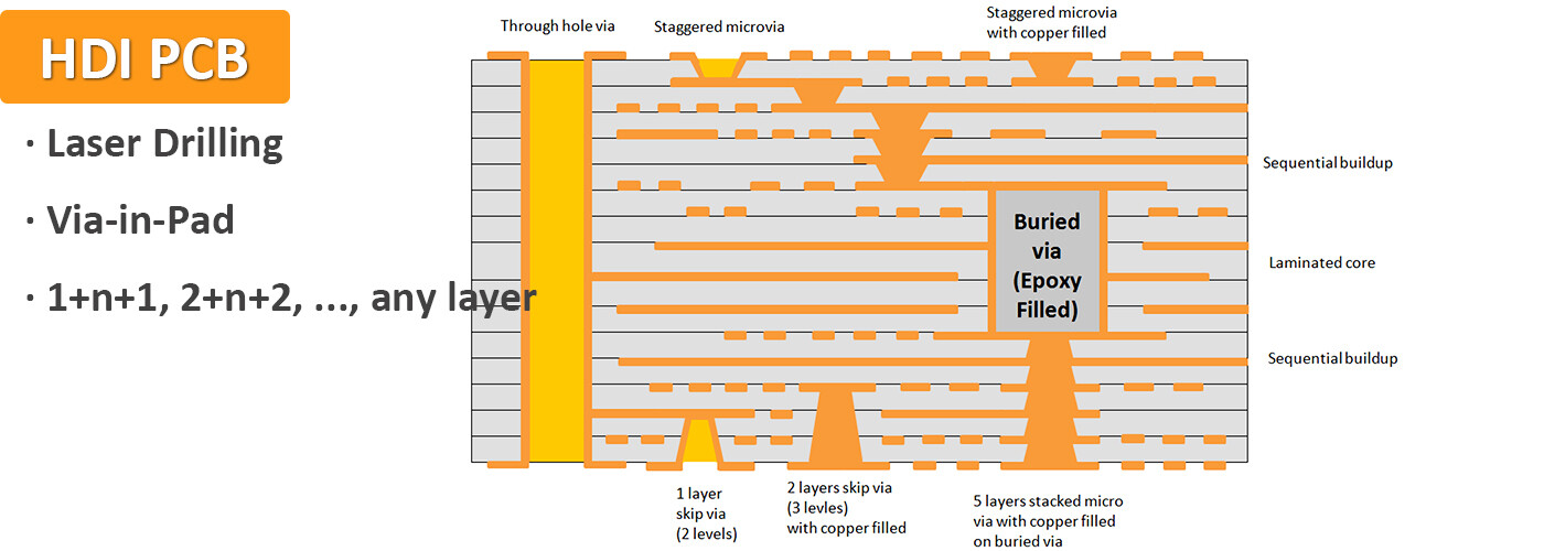
Materials used: The core material can be FR4, metal, glass fiber, or other materials. For surface treatment, you can choose ENIG, HASL, immersion tin, immersion silver, gold plating, or other types. ENIG is the most common surface treatment method for HDI due to its flatness and ease of solderability.
Multiple laminations: The number of layers and the structure of blind buried holes determine the required number of laminations. While more layers of lamination imply increased processing time and higher costs, investing in additional layers can enhance the performance and cost-effectiveness of the product.
Via-filling vs. Through-hole: There may also be cost differences between via-filling and through-hole configurations. Microvias in via-filling can be filled with copper, whereas microvias in through-holes cannot. Filling blind buried vias requires more material and time.
PAD Size: It is important to determine the size of the PAD as early as possible to help reduce costs. Understanding the appropriate PAD size will assist you in planning the design effectively and economically.
Production Cycle: Requesting an urgent PCB delivery may lead to higher costs as additional resources are required to fulfill the expedited order. Sometimes, last-minute situations arise that are beyond your control, but planning orders in advance can help improve cost efficiency. SprintPCB offers fast production lead times and customer service.
PCB Supplier: Your choice of PCB partner will significantly impact the cost of your HDI boards. You want to select a supplier that offers competitive pricing while effectively delivering high-quality products to ensure cost-effectiveness. Ordering high-quality goods is preferable to ordering parts for repair or replacement.
Compared to regular circuit boards, HDI (High-Density Interconnect) circuit boards typically have higher wiring and pad densities. They also feature smaller trace widths and spacings. These characteristics are achieved through the incorporation of techniques such as blind vias, buried vias, and microvias. These advancements in technology also make them more expensive compared to traditional circuit boards.
The three main principles for HDI PCB design are as follows:
Firstly, unlike traditional circuit boards with plated through-holes (PTH), microvias will be used. This will increase the routing density of the inner layers.
Secondly, you will have to consider a new layer stacking method that will help eliminate through-hole vias.
Thirdly, ensure that the placement of microvias allows for the creation of channels and avenues to improve routing.
The application of HDI PCB
HDI PCB is suitable for various industries. As mentioned above, you can find them in all types of digital devices like smartphones and tablets, and miniaturization is the key to their effective application. You can also find them in vehicles such as cars, planes, and other vehicles that rely on electronic products. Here are some applications of HDI PCB:
Electronic products in the automotive industry (navigation, GPS, etc.)

Smartphones and mobile phones

Laptops

Gaming consoles

Wearable technologies (Apple Watch, fitness trackers, etc.)

Telecommunications

The future development trends of the HDI industry
Although China has become the largest PCB market globally, the mainland's production capacity still primarily focuses on low-tech, low-value-added products. According to Prismark's statistics, in 2016, the mainland accounted for 19.1%, 13.5%, and 10.4% of the output value in the 4-layer, 6-layer, and 8-16-layer PCB markets, respectively. The sales volume of IC carrier boards and high-layer boards of 18 layers and above had a small share, only 2.7% and 1.2%, respectively. The market shares of HDI boards and flexible boards were 16.5% and 17.1%, respectively.
Currently, the process of survival of the fittest is accelerating in China's mainland industry, and the PCB industry is entering a phase of upgrading.High-end and cutting-edge products are still concentrated in Japan, Taiwan, South Korea, and Western Europe. From a technological standpoint, Japan remains the world's leading producer of high-end PCBs, specializing in advanced HDI boards, package substrates, and high-density flexible boards. The United States still maintains research and production capabilities for highly complex PCBs, primarily focusing on high-end multilayer boards, which are extensively used in domestic, aerospace, and communication sectors. South Korea and Taiwan have also gradually entered the competition in higher value-added areas, such as package substrates and HDI boards.
Industry demands are driving the rapid development of HDI (High-Density Interconnect) technology. Electronic products such as smartphones, tablets, and wearable devices are evolving towards miniaturization, multifunctionality, and extended battery life. Taking Apple as an example, the iPhone 4S introduced Anylayer HDI for the first time, while the iPhone X incorporated SLP (Substrate-Like PCB) technology.
The stacked SLP technology allowed the iPhone X's mainboard to be only 70% of the size of the iPhone 8 Plus's mainboard. With the upgrade to 5G communication technology, Huawei, OPPO, and vivo have extensively adopted Anylayer HDI mainboards in their 5G models, and even mainstream and low-end models have seen an increase in the HDI level of their mainboards. The evolution of smartphone mainboards has progressed from single-layer HDI to high-level and arbitrary-level HDI, and further to SLP, with continuous reduction in line width/spacing and continuous improvement in component density.
The automotive HDI (High-Density Interconnect) product space is vast. With the trend towards intelligence and automation, there is great potential for growth in the configuration and performance of vehicle domain controllers, which encompass entertainment systems, ADAS (Advanced Driver Assistance Systems), and autonomous driving systems. This growth is facilitated by an increasing number of high-speed computing chips packed within a limited volume. For instance, Tesla's ADAS controller adopts a 3rd-order 8-layer HDI design. In the future, it is expected that the development path for automotive mainboards will follow a similar trajectory as that of mobile phone mainboards, progressing from lower level to higher-level HDI processes.