Copper foil is an essential material in
PCB manufacturing, playing crucial roles in connection, conductivity, heat dissipation, and electromagnetic shielding.
Today, we'll discuss the differences between rolled annealed (RA) copper foil and electrodeposited (ED) copper foil, the various classifications of PCB copper foil, and the specialized application of thick copper PCBs, along with their manufacturing processes and design considerations.
Differences Between Rolled Annealed (RA) and Electrodeposited (ED) Copper Foils
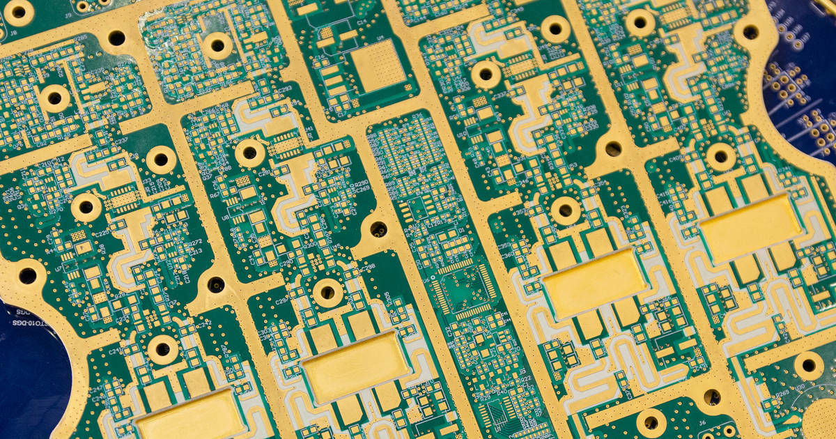
PCB copper foil is the conductive material used to connect electronic components on a circuit board. Based on manufacturing processes and performance, PCB copper foil can be classified into RA and ED types.
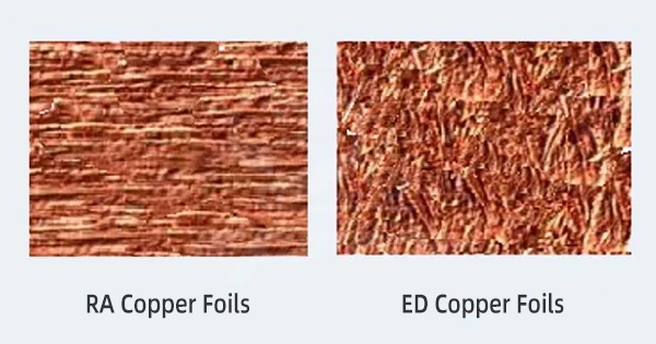
Rolled Annealed (RA) Copper Foil:
Made by rolling and compressing pure copper billets, RA copper foil features a smooth surface with low roughness and excellent conductivity, making it suitable for high-frequency signal transmission. However, RA copper foil is relatively expensive and has a limited thickness range, typically between 9-105 µm.
Electrodeposited (ED) Copper Foil:
Produced by electrolytic deposition on a copper substrate, ED copper foil has one smooth side and one rough side. The rough side bonds to the substrate, while the smooth side is used for plating or etching. ED copper foil is more cost-effective and available in a wider thickness range, typically between 5-400 µm. However, it has a higher surface roughness and lower conductivity, making it less suitable for high-frequency applications.
Classification of PCB Copper Foil
Based on the roughness of electrodeposited copper foil, it can be further categorized into the following types:
HTE (High Temperature Elongation):
Used primarily in multilayer PCBs, HTE copper foil has good high-temperature ductility and adhesion strength, with a roughness typically between 4-8 µm.
RTF (Reverse Treat Foil):
RTF improves adhesion performance and reduces roughness by adding a specific resin coating on the smooth side of ED copper foil. The roughness is usually between 2-4 µm.
ULP (Ultra Low Profile):
Made using special electroplating techniques, ULP copper foil has an extremely low surface roughness, ideal for high-speed signal transmission, with a roughness typically between 1-2 µm.
HVLP (High Velocity Low Profile):
An advanced version of ULP, HVLP is manufactured by increasing the electroplating speed, resulting in even lower surface roughness and higher production efficiency, typically between 0.5-1 µm.
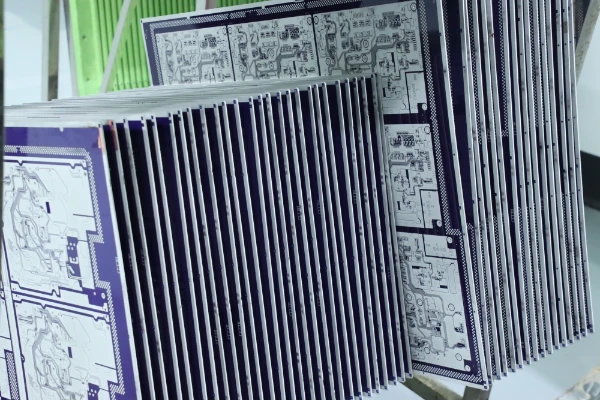
What is Thick Copper PCB?
Thick copper PCBs use base or surface copper layers exceeding 3 ounces (approximately 105 µm). These PCBs offer advantages such as handling high current loads, high-temperature resistance, robust connections, increased mechanical strength, and reduced product size.
Applications of thick copper PCBs include power supplies, welding equipment, distribution systems, power converters, solar panel equipment, medical devices, automotive, and aerospace industries.
Manufacturing Process of Thick Copper PCBs
The primary manufacturing process for thick copper PCBs involves electroplating and etching. Electroplating deposits copper to the desired thickness, followed by etching to create conductive paths.
Design Considerations for Thick Copper PCBs
Component Spacing on PCB:
Ensure proper spacing (generally > 0.5 mm) between components for electrical isolation and heat conduction.
PCB Size Requirements:
Determine the PCB size based on component quantity and layout while minimizing size without compromising thermal management.
Component Types on PCB:
Select components based on power, current, voltage, and frequency parameters to ensure performance and reliability, typically opting for high-power, high-current, high-temperature, and high-frequency components.
With 17 years of experience, SprintPCB in Shenzhen, China, offers professional and efficient PCB manufacturing services. We specialize in various types of PCBs, including
flexible-rigid PCBs, thick copper PCBs,
multilayer PCBs, and high-frequency PCBs. Whether you need PCB prototyping or mass production, we are dedicated to meeting your custom requirements!