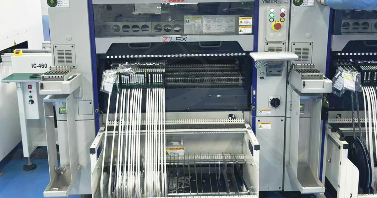
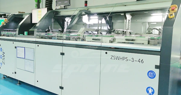
PCB (Printed Circuit Board) is an indispensable key component in modern electronic devices. Whether it's a small electronic device or a large industrial equipment, high-quality and reliable PCBs are required to ensure device performance and reliability. This article will share some successful tips and techniques for enthusiasts in the PCB industry, helping them master the art of Printed Circuit Board design and manufacturing.
Step 1: Understanding Printed Circuit Board Design Principles
Before starting Printed Circuit Board design, it is crucial to have a deep understanding of the principles behind it. Mastering the fundamentals of electrical principles, signal transmission, noise control, and electromagnetic compatibility can help designers avoid potential issues and improve design quality.
When it comes to the basics of electrical principles, signal transmission, noise control, and electromagnetic compatibility, here are some important concepts and principles.
Electrical Principles:
Voltage: Represents the potential difference and serves as the driving force for the flow of charge in a circuit.
Current: Refers to the speed at which charge passes through a conductor, representing the flow of charge in a circuit.
Resistance: Determines the degree to which current flow is impeded, measured in ohms.
Capacitance: The ability to store charges, resulting in the separation of charges between two conductors.
Inductance: The response of a conductor to changes in current, generating a magnetic field.
Signal Transmission:
Transmission Line: A wire or cable used to transmit signals within a circuit.
Bandwidth: The frequency range that a signal transmission line can transmit.
Clock Signal: A signal used for synchronizing and timing various components in electronic devices.
Serial Communication: A communication method that transmits data bit by bit.
Parallel Communication: A communication method that simultaneously transmits multiple bits.
Noise Control:
Signal Interference: Electromagnetic interference from other electronic devices or circuits that affects signal quality.
Ground Loops: Noise caused by potential differences in grounding between different locations.
Noise Suppression: The reduction of noise interference using methods such as filters, shielding, and decoupling capacitors.
Differential Signal: Reducing noise interference by combining a signal with its inverted signal.
Electromagnetic Compatibility:
Electromagnetic Radiation: Electromagnetic waves generated by electronic devices that may interfere with other devices.
Shielding: The use of metal enclosures or layers to block and isolate electromagnetic radiation and interference.
Grounding Design: Proper planning and connection of device grounding to reduce electromagnetic interference and ground loops.
A thorough understanding of these concepts will help you address issues and optimize your designs better during the PCB design and manufacturing process.
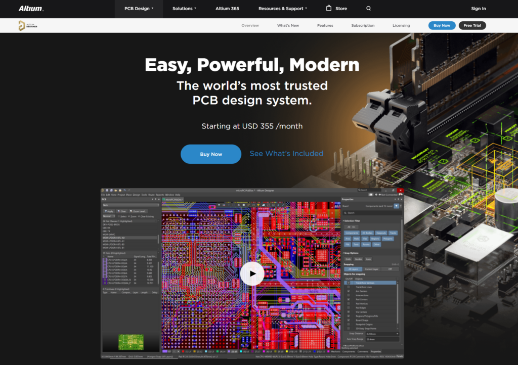
Step 2: Choosing the appropriate Printed Circuit Board design tool
Choosing the right Printed Circuit Board design tool is one of the key factors for success. There are many powerful Printed Circuit Board design software options available in the market, such as Altium Designer, Eagle, and KiCad. By selecting a tool that suits their needs, designers can efficiently complete their Printed Circuit Board design work.
Here are some advantages and disadvantages of Printed Circuit Board design software like Altium Designer, Eagle, and KiCad.
Advantages of Altium Designer:
Powerful features and comprehensive design environment suitable for complex PCB designs.
Provides a rich library and component database for convenient use by designers.
Advanced layout and routing capabilities that efficiently handle complex circuit designs.
Supports multiple file formats and integrated version control systems for easy team collaboration.
Offers comprehensive simulation and validation tools that aid in design verification and issue resolution.
Disadvantages of Altium Designer:
High cost, which may not be affordable for individual designers or small teams.
The learning curve is steep, and it takes some time to become familiar with and master the software.
Handling large-scale projects may require higher computer specifications and resources.
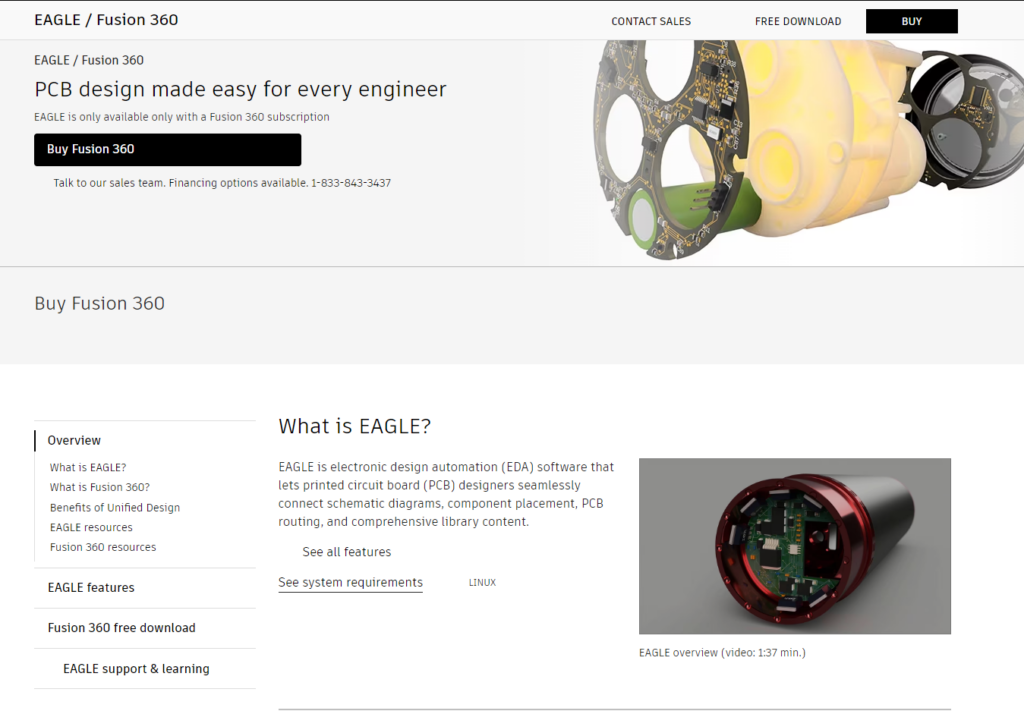
Advantages of Eagle:
User-friendly interface that is easy to learn and use.
Provides a free version suitable for individual designers or small projects.
Active user community and extensive resource support.
Good layout and routing capabilities suitable for medium-sized PCB designs.
Disadvantages of Eagle:
Performance limitations when dealing with complex and large-scale projects.
Limited functionality, lacking some advanced features and simulation tools.
Purchase of paid versions may be required for advanced features and extended functionality.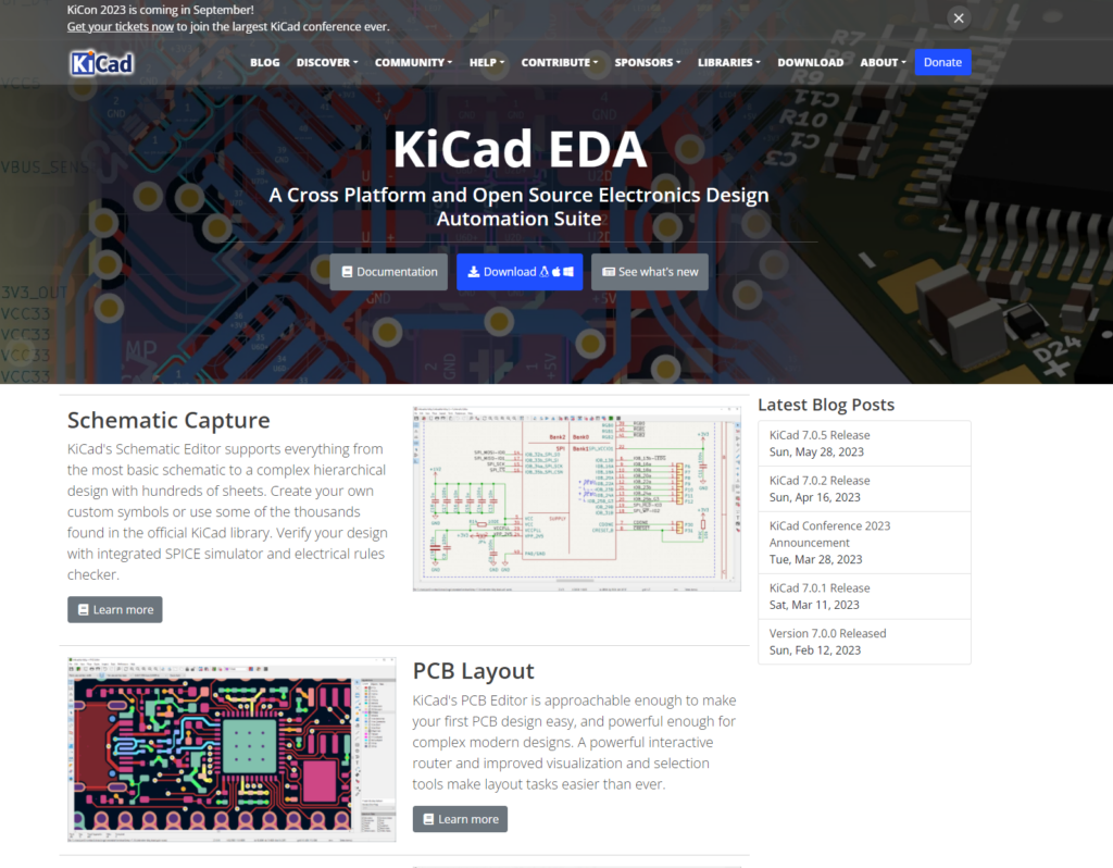
Advantages of KiCad:
Free and open-source, suitable for individual designers and small teams.
Offers stable layout and routing capabilities for medium-sized PCB designs.
Active user community and extensive resource support.
Customizable and extensible software functionality to meet individual needs.
Disadvantages of KiCad:
Steep learning curve, requiring more time to master compared to other commercial software.
Certain advanced features and simulation tools may be missing or less powerful compared to commercial software.
Lacks some advanced features like 3D visualization.
Step 3: Careful Layout and Routing in Printed Circuit Board Design
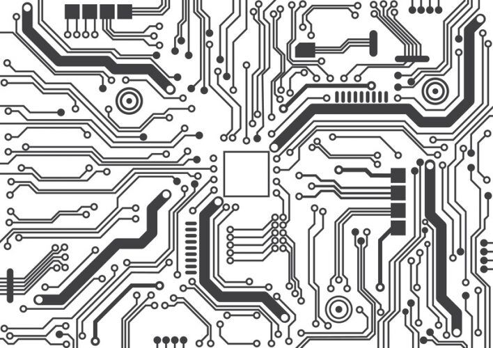
Good layout and routing can minimize signal interference and noise while improving the performance and stability of the circuit. During layout, designers should arrange component placements sensibly, pay attention to the routing of signals and power lines, and perform ground plane planning. When routing, appropriate trace widths and spacing should be used to avoid cross-interference and optimize signal integrity.
Here are some practical examples and techniques to minimize signal interference and noise, and improve circuit performance and stability during PCB layout and routing.
Separate Analog and Digital Signals: Separate the layout of analog and digital signals to avoid mutual interference. Analog signals are typically more sensitive and should be isolated from digital signals as much as possible.
Ground Plane Planning: Proper ground plane planning reduces noise and interference on the ground return path. Ensure sufficient ground plane areas and good connections to the ground pins of relevant components.
Manage High-Speed Signals: For high-speed signal lines, use techniques such as differential pairs, impedance matching, and signal length matching to maintain signal integrity. These techniques can reduce signal distortion and crosstalk, improving signal quality.
Separate Power and Signal Lines: Separate the layout of power and signal lines to minimize the impact of power noise on signals. Avoid running power and signal lines in parallel and keep them as far apart as possible.
Avoid Cross-Interference: When routing, avoid crossing signal lines. Cross-interference can cause crosstalk and electromagnetic interference, leading to degraded signal quality. Use inter-layer routing or employ vias for inter-layer connections to avoid cross-interference.
Pin Allocation Strategy: Allocate pins sensibly to keep the signal paths between relevant components as short and direct as possible. This helps reduce signal transmission delay, loss, and circuit crosstalk.
Control Impedance: Control the impedance of signal lines to match the characteristic impedance of drivers and receivers according to design requirements. Impedance mismatch can result in signal reflection and integrity issues.
Ground Pin Layout: For sensitive analog circuits, try to concentrate ground pins together to form good grounding points, reducing noise on the ground return path.
Electromagnetic Shielding: For noise-sensitive circuits or modules, electromagnetic shielding techniques can be used, such as employing shielding cans, inter-layer shielding, and ground plane isolation, to reduce the impact of external interference.
Coupling and Twisting: For signals that require coupling, such as clock signals and their corresponding ground lines, route them together in a twisted manner to minimize interference and crosstalk.
Step 4: Consider Thermal Management
Thermal management is an essential factor to consider for high-power or large Printed Circuit Board designs. Proper placement of heat sinks, cooling fans, or heat sinks is necessary to ensure that the circuit temperature remains within acceptable limits. Additionally, choosing suitable thermal materials and techniques such as heat sinks, thermal pads, and thermal grease can enhance heat dissipation effectiveness.
When it comes to thermal management in electronic devices or circuit boards, heat sinks, thermal pads, and thermal grease are common solutions. They each work based on different principles, and below is an explanation of each.
A heat sink is a metal component with high thermal conductivity, typically made of aluminum or copper. Its principle of operation involves increasing the surface area and providing a larger dissipating surface to accelerate heat conduction and dissipation.
The heat sink comes into close contact with the component requiring cooling, such as a processor or power amplifier, and transfers heat from the component's surface to the heat sink through thermal conduction.
The heat is then dissipated into the surrounding air through the larger surface area of the heat sink's fins. Heat sink design typically focuses on maximizing surface area, improving heat dissipation efficiency, and enhancing airflow convection to further improve cooling effectiveness.
A thermal pad is a soft material typically made of silicone gel or rubber with good thermal conductivity. Its principle of operation involves filling the gap between the heat source and heat sink to improve thermal conduction efficiency.
Thermal pads can be placed between electronic components (such as chips or power modules) and heat sinks. They have some compressibility, allowing them to fill irregular gaps and provide a better thermal conduction path.
The thermal conductivity of the thermal pad aids in quickly transferring heat from the heat source to the heat sink, thus achieving effective thermal management.
Thermal grease is a high thermal conductivity compound, usually made of silicone grease or metal oxides. Its principle of operation involves filling tiny gaps between the surface of electronic components and the heat sink, thereby improving the thermal conduction efficiency between the two.
The main role of thermal grease is to fill in minor surface irregularities and gaps, reducing the thermal resistance at the thermal interface and improving thermal conduction efficiency. By applying an appropriate amount of thermal grease, better thermal contact can be achieved, improving the conduction of heat from the heat source to the heat sink.
These thermal management solutions play a crucial role in electronic devices, helping to efficiently transfer heat from heat sources to heat sinks and ensuring that the device's temperature remains within a safe range.
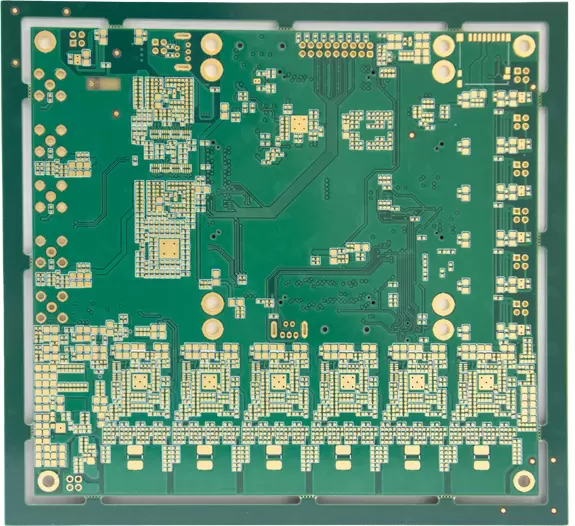
Step 5: Selecting Appropriate Materials and Manufacturers
Choosing high-quality PCB materials and reliable manufacturers is crucial for ensuring the performance and reliability of the PCB. Premium materials can provide better signal transmission and mechanical strength, while reliable manufacturers can ensure high-quality manufacturing processes and timely delivery.
Here are some well-known PCB material brands.
Isola is a global leading manufacturer of high-performance insulation substrate materials, offering a wide range of PCB material solutions.
Rogers Corporation specializes in high-performance materials, providing innovative PCB materials such as the RO4000, RO3000, and RT/duroid series for the electronics industry.

Panasonic is a renowned electronics manufacturer that also offers a variety of PCB materials, including high-performance copper foil and polyimide substrates.

Shengyi Technology is one of the leading PCB material manufacturers in China, offering a wide range of copper foils, pre-impregnated films, and substrate materials.

ITEQ is a global leading supplier of high-performance substrate materials, including glass fiber boards, polyimide boards, and multilayer materials.
Ventec International Group provides innovative PCB material solutions, including high-speed/high-frequency materials, thermal management materials, and environmentally friendly materials.
TUC is a supplier focused on rigid and flexible PCB materials, with its products widely used in automotive, communication, and consumer electronics industries.
Step 6: Conduct Rigorous Testing and Validation
Conducting rigorous testing and validation is an essential step before proceeding to mass production of the PCB. By utilizing various testing methods such as functional testing, signal integrity testing, and reliability testing, the performance of the PCB is ensured to meet expectations and potential issues are identified and addressed.
Functional testing, signal integrity testing, and reliability testing are important testing methods in PCB design and manufacturing that help ensure the performance and reliability of the PCB.
Here are some common methods and steps for these tests.
Functional testing aims to verify if the circuits and components on the PCB are functioning as expected.
These tests can be performed through the following steps.
Prepare a test plan: Determine the functions to be tested and the expected results.
Write test scripts: Prepare test scripts or test cases based on the test plan.
Set up test equipment: Acquire the necessary test equipment and tools such as oscilloscopes, multimeters, etc.
Connect test equipment: Connect the test equipment to the relevant interfaces or pins on the PCB.
Execute the tests: Follow the test scripts step by step and record the test results.
Analyze the results: Analyze the test results to confirm if the functionality is working properly.
Troubleshoot issues: If any issues are identified during the testing, trace and resolve the faults, then retest accordingly.
Signal integrity testing is used to ensure that signals are not affected by noise, distortion, or interference during their transmission on the PCB.
Here are the general steps for performing signal integrity testing.
Design a signal integrity test board: Create a dedicated board or circuit for signal integrity testing.
Define test points: Select the signal paths and test points to be tested.
Add signal probes: Connect signal probes to the test points to monitor the waveform of the signals.
Apply signals: Inject appropriate signals at the test points.
Observe signal waveforms: Use devices such as oscilloscopes or logic analyzers to observe the waveform, noise, and timing of the signals.
Analyze the results: Evaluate the signal integrity by comparing the expected signal waveforms with the observed waveforms.
Optimize the design: If any signal integrity issues are found, adjust the PCB design, such as changing the routing, adding termination resistors, or incorporating shielding.
Reliability testing aims to assess the performance and reliability of the PCB during long-term operation.
Here are some common methods for conducting reliability testing.
Temperature cycling testing: Place the PCB in different temperature environments, such as high and low temperatures, to simulate extreme operating conditions.
Vibration testing: Connect the PCB to a vibration table and subject it to vibration tests at different frequencies and amplitudes to simulate vibration environments during transportation or operation.
Humidity testing: Expose the PCB to a high-humidity environment to test its tolerance to moisture and simulate humid working conditions.
Electrical thermal stress testing: Evaluate the durability of the PCB's electronic components and solder joints by applying electrical current and conducting thermal cycling tests.
Electrical performance testing: Perform electrical parameter measurements on the PCB, such as resistance, capacitance, insulation resistance, etc., to verify compliance with specifications.
Reliability assessment: Evaluate the reliability of the PCB and identify potential issues based on the test results and specification requirements.
Mastering the art of Printed Circuit Board design and manufacturing requires continuous learning and practice.
By gaining a deep understanding of Printed Circuit Board design principles, selecting appropriate tools, conducting careful layout and routing, considering thermal management, choosing suitable materials and manufacturers, and performing rigorous testing and validation, enthusiasts in the PCB industry can enhance design quality and ensure the performance and reliability of PCBs.
By constantly striving for excellence, you too can become a master of Printed Circuit Board design and manufacturing!
Enhance Your PCB Manufacturing with SprintPCBSprintPCB is a leading high-tech company that offers top-notch PCB manufacturing services to clients worldwide. With our wealth of industry expertise and cost-effective solutions, you can concentrate on the core aspects of your business. Reach out to us now to explore the possibilities of collaboration and witness the realization of your objectives.