PCB drilling is the most expensive and time-consuming process in PCB manufacturing. The PCB drilling process must be carefully executed because even a minor mistake can lead to significant losses. The drilling process is the most critical step in PCB manufacturing. It forms the foundation for interconnections between vias and different layers, making drilling skills extremely important.
PCB Drilling Techniques
There are primarily two types of PCB drilling techniques: mechanical drilling and laser drilling.
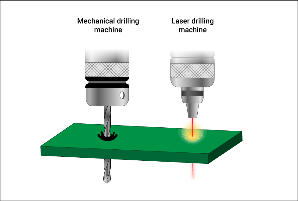
Mechanical drilling has lower accuracy but is easy to execute. This drilling technique involves using mechanical drill bits. The minimum hole size that these drill bits can produce is approximately 6 mils (0.006 inches).
Limitations of Mechanical Drilling
When used on softer materials such as FR4, mechanical drills can be used for around 800 cycles. For materials with higher density, the lifespan may decrease to 200 cycles. If PCB manufacturers overlook this aspect, it may result in incorrect holes, leading to the scrapping of the circuit board.
On the other hand, laser drilling can create smaller holes. Laser drilling is a non-contact process where the workpiece and the tool do not come into contact with each other. A laser beam is used to remove material from the circuit board and create precise holes, allowing effortless control of the drilling depth.
Laser technology is used to easily drill controlled depth vias, enabling the precise drilling of holes with a minimum diameter of 2 mils (0.002 inches).
Limitations of Laser Drilling
Printed circuit boards (PCBs) are made of copper, glass fibers, and resins, which have different optical properties, making it challenging for the laser beam to effectively penetrate the circuit board. Laser drilling, in this case, also comes with relatively higher costs.
PCB Drilling Process
For PCB engineers, understanding PCB manufacturing is essential when designing circuit boards. This ensures that the PCB design is manufacturable and reliable. Conversely, considering manufacturing processes during design can reduce costs and allow timely product delivery.
After the lamination process, the multilayered board is loaded onto the exit material panel of the drilling machine. The exit material reduces the formation of burrs. Burrs are protrusions of copper formed when the drilling axis penetrates the board. On top of this panel, more layers are stacked and carefully aligned. Finally, a sheet of aluminum foil is placed over the entire stack. The aluminum foil prevents entry burrs and dissipates the heat generated by the rapid rotation of the drill bit. Once the required number of holes is drilled, the circuit board is sent for deburring and cleaning treatment.
Due to the critical importance of drilling quality, the geometry of the tools must be considered. High-Speed Steel (HSS) and Tungsten Carbide (WC) are commonly used drill bit materials for drilling composite materials. During processing Glass Fiber Reinforced Polymer (GFRP), hard alloy tools can provide a longer tool life. Hard alloy drill bits are typically used for PCB drilling.
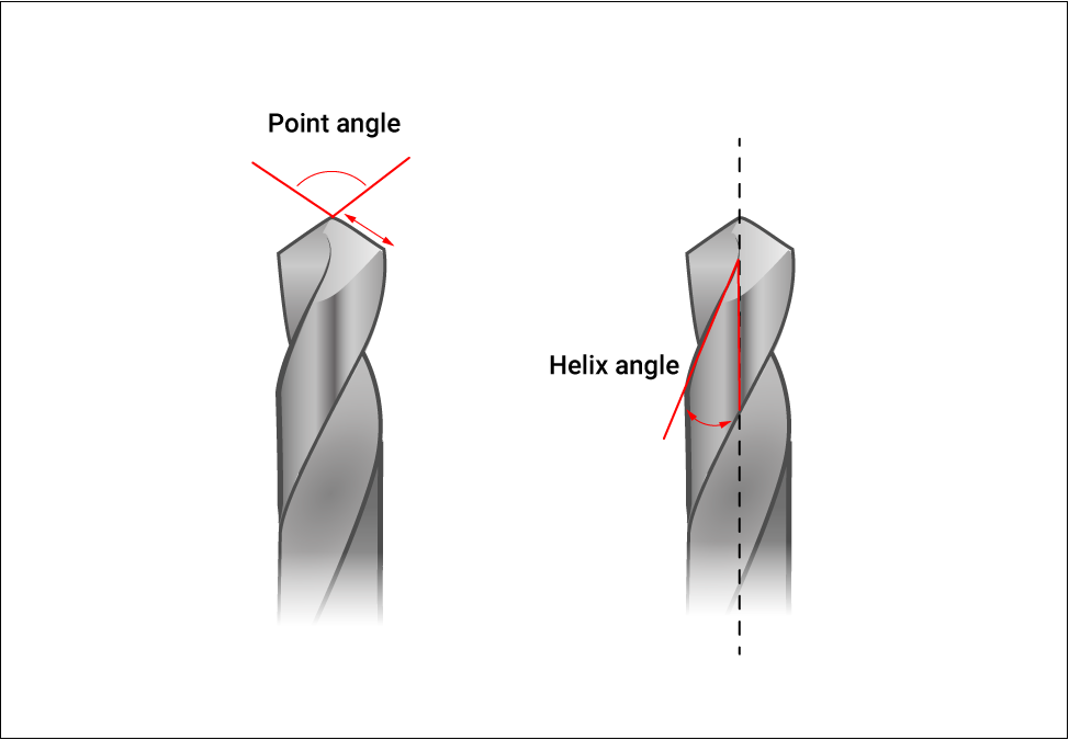
- Point angle and helix angle
The point angle of the PCB drill bit is 130°, and the helix angle is between 30° to 35°. The point angle is located at the tip of the drill bit and is measured between the most prominent cutting edges.
The helix angle is the angle on the side of the drill bit at the intersection.
- Numerical Control (NC) Drilling Machine
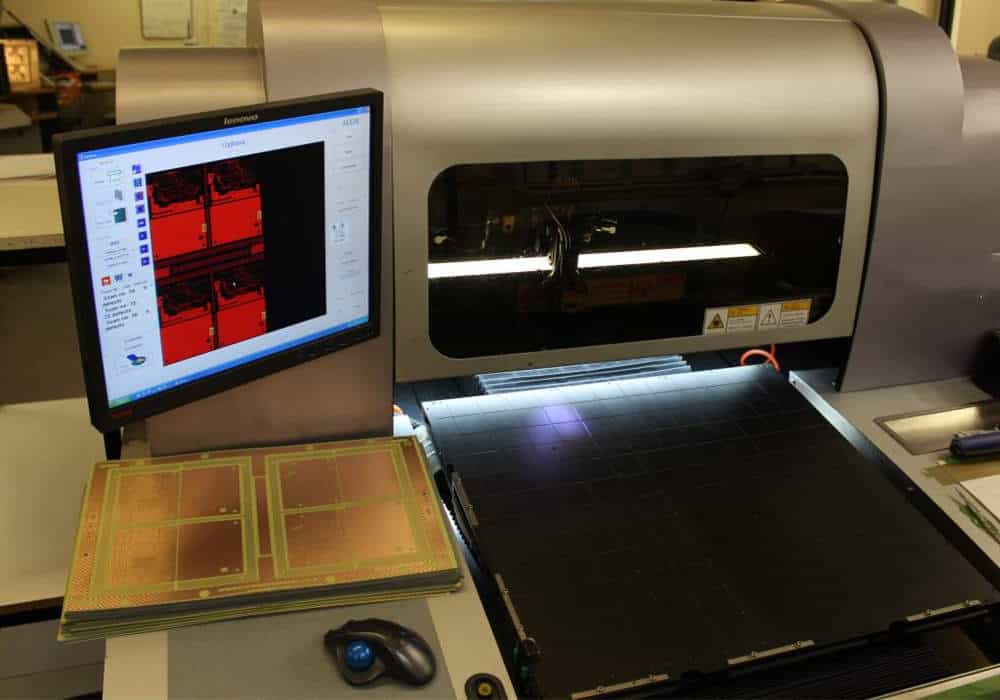
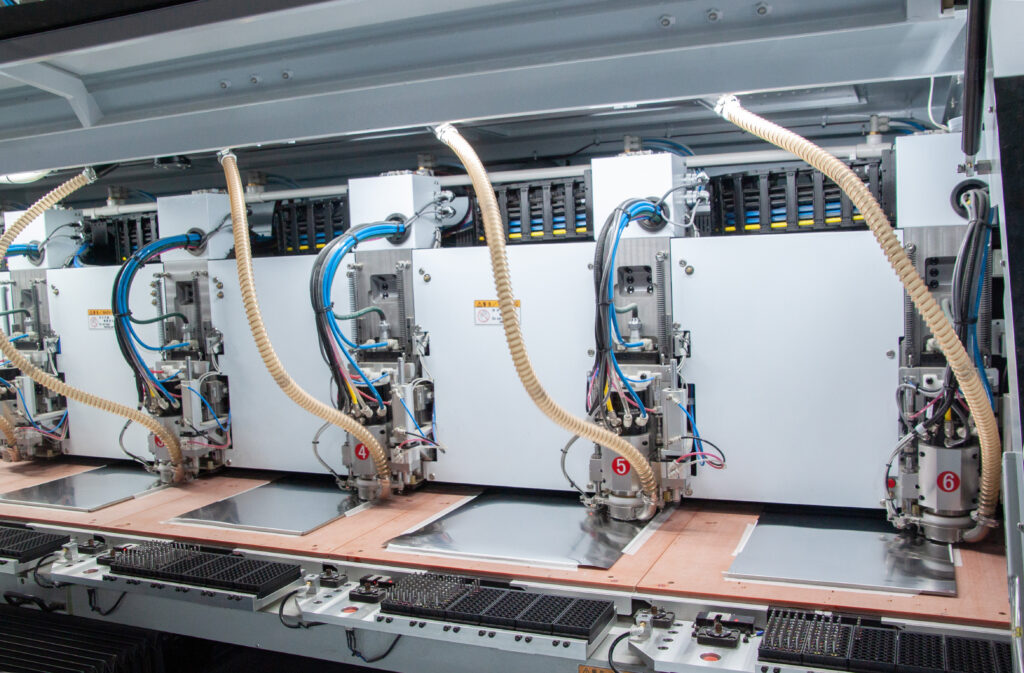
A CNC drilling machine is a pre-programmed computer numerical control (CNC) machine. Drilling is performed based on the XY coordinates input into the CNC system. The spindle rotates at a high RPM to ensure precise drilling on the board. As the spindle rotates at high speed, heat is generated due to friction between the hole wall and the spindle, melting the resin components on the hole wall and leading to resin smearing. Once the required holes are drilled, the exit and entrance panels are discarded. This is a minor detail of what happens in the workshop. Unlike etching and plating processes, drilling processes do not have a fixed duration. The drilling time in the workshop varies depending on the volume of holes to be drilled.
Two Important Aspects of PCB Drilling
The aspect ratio refers to the ability to effectively plate copper inside a hole (via). As the diameter decreases and the depth increases, plating copper inside the hole becomes a challenging task. This requires an electroplating bath with high uniform plating capability so that the liquid can flow into the tiny holes.
Aspect Ratio (AR) = (Hole Depth / Drill Diameter)
The aspect ratio for vias is 10:1, and for microvia, it is 0.75:1.
Typically, for a 62 ml PCB, the minimum drill size can be 6 mils.
Copper-Copper spacing is the planar gap between the drilled hole edge and the nearest copper feature. The nearest copper feature can be a copper trace or any other active copper area. This is a crucial factor as even small deviations can lead to circuit interruptions. The typical copper drill value is around 8 mils.
Minimum spacing = Annular Ring Width + Solder Mask Dam Spacing
Classification of PCB Drilling
Plated Through-Hole (PTH) is a conductive via that carries signals, enabling interconnections between different layers of the circuit board. It is used to securely mount components during the PCB assembly process. Non-Plated Through-Holes (NPTH) are non-conductive holes. These holes do not have tolerance levels, as components won't fit if the hole size is too large.
Drilling holes on a PCB is a challenging task that demands high precision and adherence to specific design rules.
Plated Through Hole (PTH)
Finished Hole Size (Minimum) = 0.006 inches
Annular Ring Size (Minimum) = 0.004 inches
Edge-to-Edge Spacing (from any other surface feature) (Minimum) = 0.009 inches
Non-Plated Through Hole (NPTH)
Finished Hole Size (Minimum) = 0.006 inches
Edge-to-Edge Spacing (from any other surface feature) (Minimum) = 0.005 inches
PCB Drilling Hazards
After repeated use, the drilling tools are prone to wear and breakage, leading to the following issues:
- Impaired accuracy of hole positioning
When the drill bit fails to hit the preferred point and moves along the same axis, the precision is affected. Drift in drilling can cause hole annular rings to intersect or fracture.
- Roughness inside the drilled holes
Roughness can result in uneven copper plating, leading to air voids and barrel cracks. Copper plating solution can infiltrate the hole walls, causing a decrease in insulation resistance.
Due to the heat generated during drilling, the resin in the circuit board may melt. The molten resin adheres to the hole walls, causing resin smearing. This, in turn, leads to poor copper plating and conductive faults between vias and inner layers of the circuit. Resin residues are removed using chemical solutions.
- Presence of entry and exit burrs
Burr refers to the unnecessary protrusion of copper from the holes after drilling, occurring on the top and bottom surfaces of multilayer printed circuit boards.
Inappropriate drilling conditions can cause the inner layer of copper to bend, resulting in uneven plating and conductivity issues.
Partial separation of PCB layers is known as delamination, and improper drilling can cause delamination.
Remedial Measures
This is a chemical process used to remove the melted resin deposited on the walls of holes. The process eliminates unwanted resin and enhances the conductivity through the via.
This is a mechanical process that can eliminate the raised ends (burrs) of the metal (copper), known as burrs. Any remaining fragments inside the hole are removed through the deburring process, followed by a repeated cleaning process.
Can be avoided by using laser drilling. As mentioned earlier, in laser drilling, the workpiece and the tool do not come into contact, thereby eliminating delamination.
PCB Drilling Techniques
Drilling Guide Holes for Proper Drilling
The first step before performing any drilling is to create a guide hole. This is done to prevent the drill bit from "wandering," which means the drill bit starts at one position and then moves in an unexpected direction while drilling. The guide hole can be made manually using small drill bits or automatically using a tool called a drill press.
If the guide holes are made using a drill press, the drill bits are pulled out one by one from the tool. The number of drill bits used in this process depends on the size of the PCB being drilled.
For example, if a 0.2-millimeter drill bit is used, one hole can be drilled out of four. This process usually leaves a small metal mark on the PCB when each drill bit is removed.
Use Vertical PCB Drill Bits for Drilling at an Angle
Drilling at an angle requires specialized drill bits, which are usually sold in sets and come in different sizes. The sizes include:
Wire Gauge Drill Bits: Used for wires with a thickness of 0.8 to 1 millimeter.
Small Drill Bits: Suitable for holes with a thickness or diameter ranging from 0.7 to 2 millimeters, including flat and round shapes.
Medium Drill Bits: This type is used for drilling holes with a thickness or diameter ranging from 2 to 10 millimeters, typically including flat and round shapes.
Large Drill Bits: These drill bits are used for 5 millimeters or larger holes. They can be flat or round, depending on the manufacturer.
Use the correct size of drill bits
It is essential to ensure that the drill bits used for PCB are of the appropriate size. If the drill bit is too large, it may damage the components inside the circuit board while drilling. On the other hand, if it is too small, it won't allow wires to pass through the drilled hole.
Using Drill Bits with Appropriate Speed and Power
The power and speed of the drill bit determine the drilling efficiency on metal. The most common options are:
High-speed drill bits: This type of drill bit can quickly and efficiently drill through metal, but extended use in a single session can lead to issues.
High-speed steel drill bits: These types are used for larger drilling operations and are suitable for drilling multiple, not too thick PCBs.
Plated drill bits: These drill bits are used for circuit board drilling and plating processes, as well as for drilling on thick plates or in conjunction with a high-frequency air hammer.
Using a Drilling Machine
A drilling machine is the best choice to ensure the most accurate holes are drilled. Their drilling efficiency is at least four times higher than handheld drills, and they commonly utilize industry-standard drill bits.
Understanding the operation of a drilling machine
Drilling machines vary based on their cost and capabilities, but they all work by applying the appropriate amount of pressure to drill through metal. The greater the applied pressure, the faster the drilling speed.
There are different types of drilling, such as "cross drilling," "plunge drilling," "ventilation holes," and "chamfer drilling." The most used type of drilling machine has a vertical panel (drilling into a metal plate at a certain angle). When using this type, ensure that the drill bit is facing upward and that the angle matches the holes on the PCB.
Using a drilling machine to drill PCBs
A drilling machine can be used at each stage of PCB drilling, especially when precise drilling is required. Although it takes some time to set up the drilling machine, it can yield excellent results when used correctly.
Be cautious when drilling holes
Drilling holes on a circuit board can be challenging without the appropriate tools and materials. Take your time and be patient while drilling, as rushing through the process can damage the circuit board. Always ensure that the drilling speed is neither too fast nor too slow. It is also essential to wear protective goggles while drilling to safeguard your vision.
Cleaning PCB after using the drill bit
After completing the drilling of the circuit board, it is necessary to clean the holes using a brush and solvent. The solvent will remove any metal debris that may have been generated during the drilling process on the PCB, ensuring the circuit board can be used effectively after completion.
Applying Solder to Drill Holes
After completing the PCB drilling process, you must apply solder to the new holes and melt them using a soldering iron with a small tip. To ensure proper adhesion of the solder, pass a wire through one of the holes and heat it. This will prevent the solder from dripping out of the hole. Then gently press it to ensure a secure connection.
Ensure that there are no small debris and chips on the PCB when drilling or slotting with the appropriate drill bit. If any debris or chips are found on the drill bit, it may cause issues during the drilling process and result in undesirable outcomes.
Regarding PCB drilling, if the operation is done correctly, it can be completed without damaging the drill bits. However, if mechanical parts come into contact with the drill bits during machine operation, it can cause damage to them.
DFM PCB Drilling Verification Techniques:
- The aspect ratio must be kept to a minimum to avoid drill bit wear.
- The more added drill sizesare added, the more drill bits the manufacturer will need to use. Conversely, reducing the variety of drill hole sizes will decrease drilling time.
- Confirm that you have defined the drill hole types (PTH/NPTH).
- Validate the drill hole locations/dimensions between the drill file and the factory print.
- Closed holes smaller than 0.006 inches must be dealt with.
- If drill holes and other features on the copper layer fall outside the circuit board outline, reduce the plated through-hole (PTH) size to meet the minimum aspect ratio (A/R) requirements.
- For plated through-holes (PTH) with tolerances less than +/- 0.002" and for non-plated through-holes (NPTH) with tolerances of +/- 0.001", show the arcs on the manufacturing drawing for missing NPTH drill holes/slots or notch positions from the drill file.
- Add solder to the drill holes.
- Use a precision drill press for accurate drilling.
- Clean the PCB after drilling.
Embrace innovative knowledge and elevate your PCB drilling prowess with these refined techniques. By incorporating these 9 exquisite methods into your projects, you'll unleash a world of precision and efficiency in your PCB fabrication process. Stay ahead of the curve and watch as your designs flourish with flawlessly executed drill holes, paving the way for seamless electronic connections. Start your journey towards PCB perfection today, and let innovation and expertise guide your way to unparalleled success in the world of circuitry.
Transform Your PCB Manufacturing with
SprintPCB SprintPCB is a renowned high-tech enterprise specializing in delivering exceptional PCB manufacturing services to global clients. With our extensive industry knowledge and competitive pricing, you can shift your attention towards the most vital elements of your organization. Get in touch with us today to explore the potential for collaboration and experience how we can help you surpass your goals.