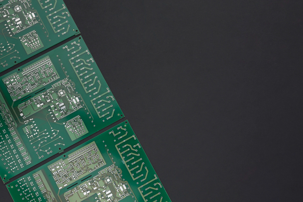
When hardware engineers first encounter multi-layer PCBs, they might feel a bit overwhelmed. Looking at ten-layer or eight-layer boards with dense, intricate traces resembling spiderwebs can leave one unsure of where to begin.
However, the design of multi-layer PCBs is an essential and integral part of modern electronic products. The internal structure of multi-layer PCBs can be represented using three-dimensional graphics, allowing people to gain a more intuitive understanding of circuit board designs.
The Core of HDI
High-Density Interconnect (HDI) is a core design for multi-layer PCBs, distinguished mainly by its via technology. The fabrication process for the circuitry in multi-layer PCBs is similar to that of single and double-layer PCBs, with the most significant difference lying in the via technology. The circuitry is etched, while the vias are formed through drilling and copper plating.
Types of Multilayer Circuit Boards
Multilayer circuit boards are common and vital components in modern electronic products. Their design and manufacturing involve selecting different layer counts and technologies based on the complexity and performance requirements of the products. The following are several common types of multilayer circuit boards and their typical applications:
Through-hole PCB
Through-hole PCB is the simplest type of multilayer circuit board, typically composed of two layers interconnected through through-holes. This type of circuit board is suitable for some simple 8-bit microcontroller products, offering a relatively lower cost. However, due to potential signal interference and design limitations caused by through-hole connections, it has gradually been replaced by other types for products with higher performance requirements.
First Order Board
A First Order Board is a common 4-layer to 6-layer through-hole board suitable for 32-bit microcontroller-level smart hardware. It provides more interlayer connection space and design flexibility, helping to reduce signal interference, providing better electrical performance, and noise immunity. At the same time, the manufacturing process is relatively simple, and the cost is relatively low, making it a preferred choice for many medium complexity products.
Second Order Board
A second order board is a more advanced type of multi-layer circuit board, typically ranging from 6 to 8 layers. The design of this board is more complex and is suitable for smart hardware at the level of Linux and Android. In these products, the layout of communication interfaces, high-speed signals, power, and ground layers requires greater precision, and using a second order board can better meet these requirements.
Second-order stacked via PCB
The second-order stacked via PCB is a complex type used in eight layers or more boards. It combines the features of first-order and second-order boards, allowing multiple vias to be placed at the same location, providing higher connection density and improved signal integrity. However, due to its complexity and manufacturing difficulty, its usage is limited and primarily applied in high-end sophisticated products.
Third-order boards and higher-order circuit boards
Third-order boards and higher-order circuit boards are typically used for extremely high-performance applications such as servers, high-end computers, etc., due to their complex design and manufacturing costs. These boards offer more layers of signal and power planes, enabling them to meet the demands of complex signal transmission and power management requirements. Due to their expensive price, they are generally utilized in applications that require extremely high performance and reliability.
Smartphones and other compact products typically adopt 8-layer first-order to 10-layer second-order circuit boards. Due to the need to accommodate numerous features and complex circuits within limited space, using more layers and higher-level circuit boards allows for better signal integrity, power management, and heat dissipation requirements.
Overall, selecting the appropriate type of multilayer circuit board depends on the product's performance requirements, signal integrity, electrical performance, layout complexity, and budget constraints. With the continuous advancement of technology, an increasing number of products will adopt higher-level circuit boards to meet the ever-growing functional and performance demands.
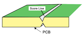
The most common type of through-hole
There is only one type of via, going from the first layer to the last layer. Whether it's an external trace or an internal trace, the via is drilled through, known as a through-hole PCB. The number of layers has no relation to through-hole PCBs; even 2-layer PCBs commonly used have through-holes. Many switches and circuit boards, despite having 20 layers, still utilize through-hole vias. The process involves drilling the PCB with a drill bit and then plating copper inside the holes to create electrical connections.
It should be noted that the plated through-hole diameters are typically 0.2mm, 0.25mm, and 0.3mm. However, the 0.2mm ones are generally more expensive than the 0.3mm ones. This is because the thinner drill bits are more prone to breakage and drilling takes longer. The additional time and drill bit costs are reflected in the increased circuit board prices.
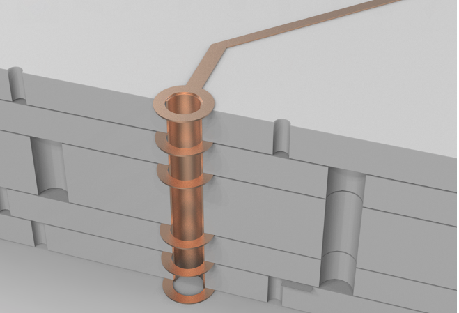
Laser vias on HDI boards
This diagram represents the layer stack-up of a 6-layer 1-order HDI (High-Density Interconnect) board. The top and bottom surfaces have two layers each with laser vias of 0.1mm in diameter. The inner layers have mechanical vias, creating a structure similar to a 4-layer through-hole board, with an additional 2 layers covering the outside.
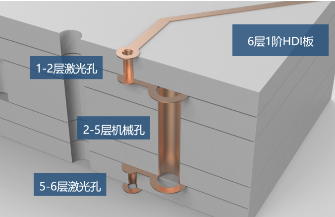
Laser vias can penetrate glass fiber materials but not metal copper. As a result, the vias on the outer layers do not affect the internal routing. After laser drilling, the holes are copper-plated, creating laser micro-vias.
2-layer HDI board with dual-layer laser
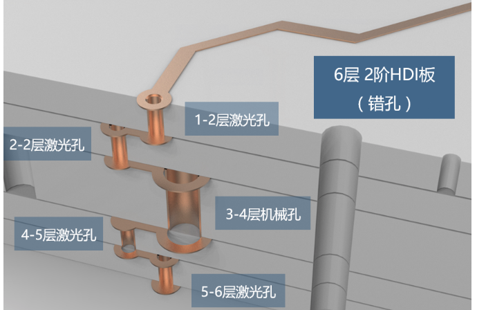
The image above shows a 6-layer 2-step staggered hole (HDI) board. Typically, 6-layer 2-step HDI boards are less commonly used, and most often, 8-layer 2-step HDI boards are preferred. However, the principles are the same when dealing with higher layer counts as in the case of the 6-layer HDI. The term "2-step" refers to the presence of two layers of laser-drilled holes. The term "staggered" indicates that the two layers of laser-drilled holes are misaligned.
Why are the holes staggered?
This is because during the copper plating process, the holes might not be fully filled, leaving voids inside the holes. Therefore, it is not possible to directly drill on top of these voids. Instead, the holes must be staggered at a certain distance, and another layer of voids is created on top.
6-layer 2-step HDI means that there are 4 layers with 1-step HDI construction, and then an additional 2 layers are added on the outside.
8-layer 2-step HDI means that there are 6 layers with 1-step HDI construction, and then an additional 2 layers are added on the outside.
Micro-via technology involves complex processes and higher costs, where two layers of laser-drilled vias overlap. This allows for more compact circuitry. The inner layer vias need to be filled with electroplating before creating the outer layer vias. This process makes it more expensive than conventional through-hole boards.
For ultra-expensive high-density interconnect (HDI) boards: it involves multiple layers of laser-drilled micro-vias. Each layer consists of laser-drilled vias, providing the flexibility to route and create vias as desired.
The Layout Engineer is extremely satisfied and fulfilled with their work! They no longer have to worry about being unable to create the ideal design. However, the Procurement Department is facing significant pressure because the cost of the Any-Layer HDI (High-Density Interconnect) board is more than 10 times higher compared to regular through-hole boards!
This also explains why only high-end products like the iPhone can afford to use such expensive boards. Currently, it seems that other mobile phone brands have not heard of anyone adopting the Any-Layer HDI board.
SprintPCB: Your Reliable PCB Support Provider
SprintPCB is a renowned high-tech enterprise offering comprehensive PCB manufacturing services to clients globally. With our extensive expertise and cost-effective solutions, you can prioritize your organization's critical requirements while enjoying a seamless process. Get in touch with us today and discover how we can assist you.