What is PCB Dry Film?
Dry film, in contrast to wet film, is a polymer material that, when exposed to UV light, undergoes a polymerization reaction to form a stable substance adhered to the board surface, blocking plating and etching. PCB dry film is a crucial material in
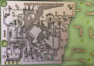
PCB manufacturing, where specific processes transfer circuit patterns precisely onto copper plates.
The dry film mainly consists of a polyester film and a high-sensitivity adhesive that responds to UV light to create fine images. It is a photosensitive material, and through exposure, development, and etching, it forms accurate circuit patterns on copper foil, making it ideal for high-precision circuit board manufacturing. Dry films provide high resolution, supporting intricate circuit designs with exposure reactions at fine line widths and spaces down to 50µm.
The functions of dry film are to form circuit patterns and provide plating resistance and hole sealing.
Common thicknesses include 0.8 mil, 1.2 mil, 1.5 mil, and 2.0 mil.
PCB Dry Film Process
Film Application:
The first step is to apply the dry film onto the copper plate. This involves firmly attaching the dry film to the copper surface of the circuit board. The dry film acts like a protective layer, covering the entire copper surface. A laminating machine applies pressure and a temperature of 110°C to ensure the dry film is well adhered, preventing any misalignment or errors during subsequent exposure.
Exposure:
The next step is exposure, which "prints" the pattern onto the dry film. A photomask, with the circuit design, is placed over the dry film. UV light passes through the transparent areas of the photomask to expose the dry film. The exposed areas undergo a chemical change and become hard, while the unexposed areas remain soft, effectively "engraving" the circuit design onto the dry film.
Development:
The development step removes any excess dry film. A developer solution, usually 1% potassium carbonate or sodium carbonate, dissolves the unexposed areas of the dry film, revealing the pattern. After this step, the circuit design clearly appears on the board, as though the dry film has "sculpted" the circuit lines.
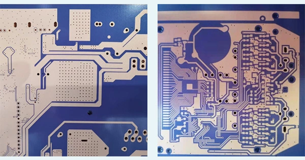
Etching - Forming Circuit Patterns:
The final etching step is like the "final cleanup." An etchant, typically acidic (sodium hypochlorite + HCL) or alkaline (ammonia + ammonium chloride), removes the exposed copper. The dry film protects the exposed areas, so the etchant only removes the unprotected copper, leaving the desired circuit intact.
Film Removal:
Finally, the dry film is removed, revealing the complete circuit. This is typically done with a 3-5% sodium hydroxide solution heated to 50°C, completely exposing the circuit.
Common Issues and Solutions in PCB Dry Film Usage
Bubbles Between the Dry Film and Copper Foil Surface
Issue: Bubbles can affect subsequent exposure and etching, leading to unclear circuit patterns.
Solution: Ensure the copper foil surface is smooth and even. Increasing the pressure during lamination can effectively reduce bubble formation. Handle boards gently, avoiding excessive force during lamination. Regularly inspect and maintain the smoothness of hot rollers to prevent dents or contamination. Also, try lowering the lamination temperature to reduce wrinkling caused by temperature differences.
Exposure Issues
Issue: Insufficient exposure results in blurry patterns and unclear lines, while overexposure can fully cure the dry film, making it impossible to develop the desired pattern.
Solution:
For underexposure: Increase exposure time or the light source’s intensity to ensure sufficient UV exposure for the dry film. Regularly check the light source for normal operation and replace aging bulbs.
For overexposure: Decrease exposure time or adjust the distance between the light source and the dry film. Follow recommended exposure parameters strictly to maintain consistency.
Development Issues
Issue: During development, unclear patterns, missing lines, or uneven development may occur.
Solution:
For incomplete development: Extend development time or increase developer temperature to help dissolve the dry film more effectively. Ensure the developer’s concentration is appropriate, as low concentration can lead to poor development.
For overdevelopment: Reduce development time, control the temperature, and monitor the developer’s concentration. Maintain developer quality by replacing solutions that have been used for extended periods.
Insufficient Adhesion of Dry Film to Copper Foil
Issue: If the dry film is not firmly adhered to the copper foil, subsequent processes may encounter issues.
Solution: Clean the copper foil surface thoroughly to avoid any residues of grease or oxidation. Use gloves to ensure the dry film remains clean and choose high-quality dry film within its shelf life to avoid unnecessary problems. Adjust lamination speed and temperature, and keep the humidity in the production environment around 50% to improve dry film adhesion.
Wrinkling of Dry Film
Issue: Wrinkles not only affect appearance but may also interfere with the circuit pattern.
Solution: Wrinkling usually results from overly adhesive dry film or improper handling. Handle boards carefully to avoid pressing or bending them forcefully. Additionally, lowering the preheating temperature of the board can help reduce the risk of wrinkling.
Residual Adhesive
Issue: Residual adhesive affects both appearance and circuit performance.
Solution: Residual adhesive is often caused by poor dry film quality, excessive exposure time, or ineffective developer solution. Resolve this by using high-quality dry film, adjusting exposure time, and refreshing the developer solution. Following standard procedures can also greatly reduce residual adhesive issues.
By paying attention to these details and promptly adjusting and optimizing the process, most issues encountered with dry film usage can be resolved, leading to improved PCB quality.