In the modern electronics industry, PCB delivery time is a crucial challenge. With advancing technology and intensifying market competition, the demand for high-quality PCB products has become increasingly urgent. This challenge is particularly significant in the realm of complex PCB designs. Customers expect to receive finished complex PCBs in the shortest possible time to meet the growing market demands and rapidly evolving innovative designs.

Therefore, we are faced with a crucial question: Can complex PCBs be delivered in 7 days or less? This article will delve into the challenge of PCB delivery and provide factual evidence through real-life examples. We will explore potential solutions and innovative technologies that can enable faster, more efficient, and reliable PCB delivery. Whether you're a time-constrained business or a reader interested in PCB delivery times, this article will provide you with valuable insights and practical advice. Let's explore the possibilities of delivering complex PCBs within strict time requirements.
Complex PCB designs face many challenges that require designers and manufacturers to employ special strategies and techniques to overcome. Firstly, complex PCBs often have multiple layers. Compared to traditional double-sided or four-layer PCBs, multi-layer PCBs have a more intricate structure to accommodate more signals and power planes. Such designs present challenges in wiring and layout as they require higher wiring density and interlayer connections. Secondly, complex PCBs often involve dealing with high-density routing. As electronic devices become smaller, lighter, and more powerful, there is an increasing demand for tight component placement on PCBs. This has led to more intricate routing tasks, including fine line widths, small spacing, and components with tiny packages. These requirements add complexity and difficulty to the routing process, while also increasing the potential for issues during the design and manufacturing stages. In addition, the demand for complex PCBs is also related to the application field. For example, the requirements for PCBs are increasing in areas such as telecommunications equipment, medical devices, and industrial automation. In telecommunications equipment, there is a need for high-speed data transmission and stable signal integrity. Medical devices may require handling precise sensors and complex control circuits. Industrial automation systems need to withstand harsh environmental conditions while maintaining reliability and stability. These requirements make complex PCB designs necessary, while also adding pressure to the delivery time. To address these challenges and requirements, designers and manufacturers need to employ a range of strategies and technologies to optimize the design and manufacturing process of complex PCBs. This may involve using advanced design software and tools to support multilayer designs and high-density routing. Additionally, conducting signal integrity analysis and electromagnetic compatibility design ensures the reliability and performance of the circuits. Furthermore, close collaboration and communication are crucial to identify and resolve potential issues early on.
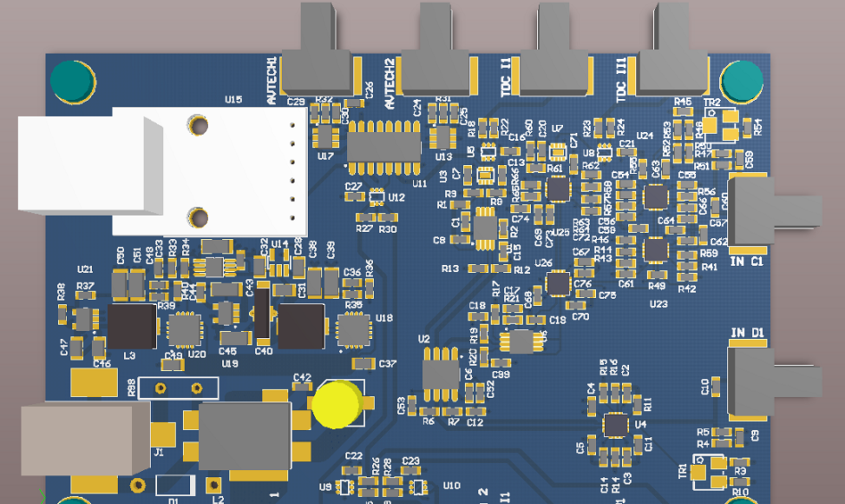
For example, modern PCB design software such as Altium Designer, Cadence Allegro, and Mentor Graphics PADS offer powerful features and user-friendly interfaces that help designers work more efficiently in complex PCB design processes. These software solutions provide advanced layout and routing tools that can automatically perform rule checks, signal integrity analysis, and electromagnetic compatibility validation to ensure design accuracy and reliability.
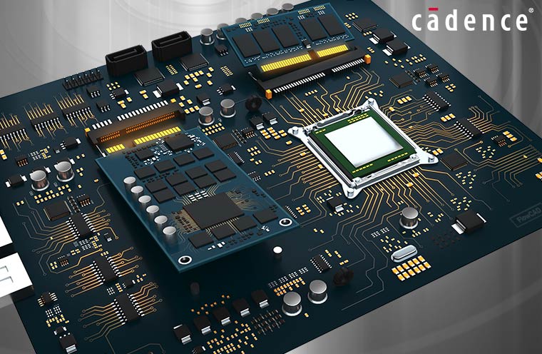
Another example is simulation tools like SPICE simulators and high-frequency electromagnetic simulation software. These tools can simulate the performance and behavior of circuits, aiding designers in identifying and addressing potential issues during the design phase. By conducting signal integrity simulations and electromagnetic compatibility simulations, designers can predict and correct factors that may cause signal distortion, crosstalk, or interference, thereby enhancing the performance and reliability of the PCB design. In addition, advanced PCB design tools also support 3D layout and package design. Designers can use 3D CAD tools to visualize the layout of the PCB, ensuring accurate component placement and space utilization. At the same time, package libraries and package editors allow designers to select and customize packages suitable for complex PCBs, meeting the requirements of high-density routing and miniaturization.

In the challenge of PCB delivery, optimizing the PCB design is a crucial step that can significantly reduce delivery time and enhance production efficiency. Here are some effective methods and practices that can be employed to expedite the PCB design and delivery process. First, reasonable layout planning is the key. By carefully planning component placement and routing paths, signal interference and EMI problems can be reduced, reducing the need for subsequent debug and repair. For example, in PCB design for high-speed signal transmission, key signal lines are placed on short and direct paths to reduce transmission delay and signal distortion. Optimizing the layout can also reduce the physical size of the PCB, thereby reducing manufacturing costs and material waste. Second, performing signal integrity analysis is an important step in ensuring a high-quality design. Using professional PCB design software and simulation tools, it is possible to simulate and evaluate circuit performance and detect potential signal integrity issues such as reflections, crosstalk, and timing skew. By identifying and addressing these issues early, the need for subsequent rework and repairs can be reduced, resulting in faster delivery times. In addition, electromagnetic compatibility (EMC) design is also an important aspect of optimizing PCB design. Measures such as reasonable ground wire layout, power filtering and shielding technology can effectively reduce electromagnetic radiation and sensitivity problems and ensure the normal operation of PCB in the electromagnetic environment. An optimized EMC design can reduce the time for subsequent debugging and repair, while improving product reliability and compliance. A practical case is given to support the effectiveness of these optimization methods. A communications equipment manufacturer needed to quickly deliver a PCB for a high-frequency wireless communications module. Through optimized layout and signal integrity analysis, the design team successfully reduced signal transmission delay and noise interference, which improved the performance of the module. At the same time, they have adopted professional EMC design technology to ensure the stable operation of the module in the electromagnetic environment. Thanks to these optimization measures, the manufacturer is able to successfully produce and deliver high-quality PCB modules within strict delivery deadlines. By optimizing PCB design, rationally planning layout, performing signal integrity analysis and electromagnetic compatibility design, the time for design rework and repair can be greatly reduced, thereby accelerating the delivery time of PCB. These practices not only improve PCB performance and reliability, but also help manufacturers launch new products faster and meet customer demands in a highly competitive market.

Collaboration and supply chain optimization play a key role in achieving an efficient PCB delivery process. Through close cooperation with suppliers, manufacturers and assemblers, the synergy of all links can be ensured to maximize production efficiency and delivery speed. First, collaborative cooperation with suppliers is crucial to obtain high-quality PCB key materials. Establishing a stable cooperative relationship with suppliers and timely communicating of the specifications, delivery time and quantity of required materials can avoid delays and quality problems. In addition, sharing project requirements and technical specifications with suppliers can lead to more accurate quotations and delivery commitments, leading to better planning of production schedules. Second, collaboration with manufacturers is key to ensuring efficient operation of the PCB manufacturing process. Communicating PCB design and layout requirements with manufacturers early on can avoid potential manufacturing issues and allow for feasibility assessments prior to manufacturing. In addition, sharing design files and detailed process requirements with manufacturers can ensure that the PCB manufacturing process is performed as expected, reducing the need for adjustments and repairs, thereby reducing lead times. Finally, collaboration with the assembler is key to ensuring a smooth PCB assembly and testing process. Sharing the design files and assembly requirements with the assembler can ensure that the PCB layout meets the assembly requirements and solves possible problems in advance. Additionally, timely communication of requirements and schedules regarding assembly and testing can coordinate production planning and ensure timely delivery of assembled PCBs. A successful case is a company that established a close cooperative relationship with its supply chain partners under the urgent delivery requirements. Through regular meetings and communication, they can obtain key materials provided by suppliers in a timely manner, and work with manufacturers to solve design and manufacturing problems. In addition, close collaboration with assemblers ensures efficient PCB assembly and testing. Finally, they succeeded in completing the production and delivery of the complex PCB in a short time. Through collaborative cooperation and supply chain optimization, efficient communication and coordination among all parties will reduce time delays, reduce errors and duplication of work, and increase the reliability and speed of the entire PCB delivery process. This collaborative model will create more efficient and sustainable delivery solutions for the PCB industry, which promote the development and innovation of the industry.
In PCB delivery challenges, adopting some best practices can help us better cope with time pressure and improve delivery efficiency. First, it is important to establish an efficient project management process. This includes ensuring that the project team has clear lines of communication, defined milestones and delivery timelines, and appropriate resource allocation. Delivery delays and errors can be minimized through effective project management.

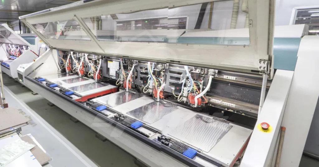
Second, adopting advanced manufacturing and testing equipment is also the key to shortening delivery time. With the continuous advancement of technology, modern manufacturing equipment can provide faster production speed and higher production capacity. Automated production lines and advanced testing equipment can reduce human errors and improve the precision and efficiency of manufacturing and assembly. Furthermore, by implementing a quality control and inspection process, it can be ensured that the delivered PCBs meet high quality standards. Another important practice is to cultivate a professional technical team. Expertise and skills in the field of PCB design and manufacturing are essential to deliver complex PCBs quickly and accurately. Ongoing training and learning programs help the technical team stay updated and abreast of the latest design and manufacturing techniques. At the same time, encouraging cooperation and knowledge sharing among team members can speed up the problem-solving and decision-making process, further improving delivery efficiency. In addition to best practices, future development trends also provide more opportunities and challenges for PCB delivery. One promising trend is the application of augmented reality (AR) technology in PCB manufacturing. By using AR technology, manufacturing personnel can view the layout, assembly, and connection information of PCBs in real time through head-mounted displays or smartphone applications. This increases the accuracy and speed of production and reduces human error. In addition, further advances in automation will also have a positive impact on PCB deliveries. With the development of machine learning and artificial intelligence technology, more manufacturing processes can be automated and intelligent, thereby reducing human intervention and speeding up delivery. For example, automated part inspection and quality control systems can quickly identify and correct manufacturing issues, improving overall delivery efficiency. Although delivering complex PCBs in 7 days or less remains a challenge, we are moving towards this goal through optimized designs, adoption of rapid manufacturing techniques, and collaborative collaboration and supply chain optimization. Through continuous efforts and innovation, we are expected to deliver high-quality complex PCBs in a shorter time, driving the development and innovation of the electronics industry.

Customer support