In the field of electronic manufacturing, Printed Circuit Boards (PCBs) have become essential components of various electronic devices. Serving as substrates that connect and support electronic components, PCBs bear crucial functions in circuitry and signal transmission. However, with the continuous evolution and increasing complexity of electronic products, manufacturing high-quality, high-performance PCBs has become more challenging. Even minor defects or errors could potentially result in equipment malfunctions, performance degradation, or even jeopardize user safety.
In this context, the emergence of Automated Optical Inspection (AOI) technology has become crucial. With its characteristics of high efficiency, accuracy, and automation, AOI technology has become an indispensable component of the modern PCB manufacturing process. It plays a significant role in achieving PCB quality assurance, defect detection, and manufacturing efficiency enhancement.
Looking back, traditional PCB quality inspection has primarily relied on manual visual inspection. However, as the complexity and density of PCBs continue to increase, the limitations of manual inspection are gradually becoming evident. Minute soldering defects, component misplacements, shorts, opens, and other issues are difficult to accurately detect at a 100% rate on fast-paced production lines. If these issues go unnoticed, they may lead to serious consequences during subsequent production and usage, thereby impacting the reliability and performance of the product.
It is precisely under the impetus of such demand that automated optical inspection technology emerges.
The emergence of AOI technology has bridged the gap left by traditional manual inspection, heralding a revolution in the PCB manufacturing industry. It has not only elevated the capabilities of quality assurance but also reduced defect rates, lowered production costs, and furnished robust assurance for the reliability and performance of electronic products.
In the following article, we will delve into the operational principles, advantages, application domains, and future developmental trends of AOI technology.
What is the working principle of Automated Optical Inspection (AOI)?
When it comes to the working principles of AOI, we delve into a highly technological field. The essence of this technology lies in the utilization of high-resolution cameras, light sources, and advanced image processing algorithms to achieve rapid and precise detection and analysis of various components, solder joints, and connections on printed circuit boards.
Cameras and Light Sources: Capturing Details
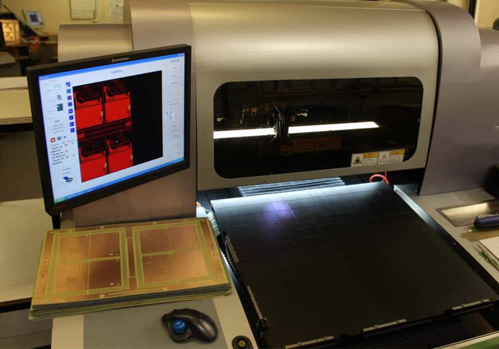
Key components of the AOI system include high-resolution cameras and light sources. The cameras are positioned at specific angles to accurately capture images of the PCB surface. The light sources provide the necessary illumination for the cameras to ensure clear presentation of details on the PCB. The synergy between these two elements allows the AOI system to capture minute and imperceptible issues such as solder joint defects, component misplacements, and short circuits.
Image Capture and Transmission: Digital Data
Once the camera captures images of the PCB surface, these images are digitized and transmitted to the connected computer system. Image transmission is typically carried out through high-speed data transfer interfaces to ensure swift and stable data transmission.
Image Processing Algorithms: Intelligent Analysis
Image processing algorithms are one of the key components of AOI technology. These algorithms possess a high degree of intelligence, capable of automatically identifying and analyzing various elements within images. They can detect the presence, position, orientation, and size of components, identify whether solder joints are correctly welded, and detect issues such as short circuits and open circuits.
These algorithms rely on predefined standards and parameters for assessment, to determine the presence of defects or errors.
Comparison and Determination: Automated Decision-Making
Once the image is processed and analyzed, the system will compare it against pre-established standards. If any deviations from the standards are detected, the system will automatically trigger an alert, notifying operators or the production team. This automated decision-making process significantly enhances production line efficiency and consistency, reducing the need for manual intervention.
Results and Reports: Data Visualization
The AOI system can generate comprehensive inspection reports, encompassing detection outcomes for each PCB, problem types, and corresponding locations. These reports hold significant value for quality control and subsequent enhancements, as they aid manufacturers in issue tracking, trend analysis, and the implementation of appropriate corrective measures.
The collaborative interaction of these components enables the AOI system to detect issues efficiently and accurately on the PCB, ensuring consistency and reliability in manufacturing quality.
Advantages of Automated Optical Inspection (AOI) Technology
High-speed Continuous Inspection
Automated Optical Inspection (AOI) technology boasts remarkable inspection speed that far surpasses the capabilities of manual inspection. During the PCB manufacturing process, a significant number of circuit boards can be produced every minute.
Traditional manual inspection methods could consume considerable time, whereas AOI technology can swiftly scan the entire circuit board in a very short span and rapidly detect any potential defects. Consequently, manufacturers can expedite production and enhance manufacturing efficiency.
Micro Defect Detection
Various minor defects exist during the PCB manufacturing process, such as soldering issues, component misplacements, and short circuits. These problems might be hard to discern with the naked eye, but they can have a significant impact on the performance and reliability of the circuit board.
AOI technology, with high-resolution cameras and precise image processing algorithms, can accurately capture these minute defects. By detecting and rectifying them promptly, manufacturers can ensure the quality and reliability of the final product.
Automation and Consistency
The automated features of AOI technology imply a minimal level of human intervention on the production line. Conventional manual inspections can be influenced by operator skill levels and fatigue, leading to inconsistent outcomes.
In contrast, AOI systems maintain consistency in performing the same tasks, whether it is day or night, during peak hours or off-peak periods. This consistency aids in reducing the number of defective products and enhancing product reliability.
Data-Driven Decision Making
AOI technology is not only limited to detecting issues; it also generates substantial amounts of data and images, providing manufacturers with valuable insights. This data can be utilized to analyze trends and patterns on the production line, assisting manufacturers in identifying potential sources of problems and implementing preventive measures.
Through data analysis, manufacturers can gain a better understanding of vulnerabilities within the production process and pursue continuous improvement.
Reducing Costs and Human Errors
The implementation of automated optical inspection technology contributes to mitigating the risks associated with manufacturing costs and human errors. By minimizing the quantity of defective products and the time required for manual operations, manufacturers can decrease scrap rates and production costs while maintaining high quality.
Furthermore, automated optical inspection technology can also diminish issues stemming from human oversight or errors, thereby enhancing overall operational efficiency.
AOI Applications and Challenges
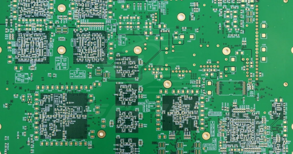
Automated Optical Inspection (AOI) technology finds extensive applications in the field of PCB manufacturing. It spans various stages from initial soldering to final assembly, ensuring the quality and consistency of the entire manufacturing process. The following are some typical application areas:
Welding Inspection
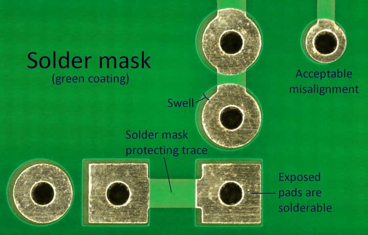
During the soldering phase in PCB manufacturing, automated optical inspection technology can assess the quality of solder joints, detecting factors such as uniformity, the presence of bubbles, or cracks. This is crucial for ensuring the reliability and stability of soldered connections.
Component Assembly
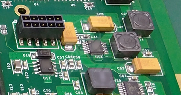
During the PCB assembly process, automated optical inspection (AOI) technology is employed to verify the position, orientation, and alignment of components, ensuring their full adherence to design specifications. This aids in preventing incorrect component placement, thereby mitigating potential issues that could lead to failures.
Trace Tracing and Connectivity
Automated optical inspection technology can detect whether the traces on the PCB are connected, as well as whether there are any short or open circuits. This helps ensure the proper functioning of the circuit board and prevents any electrical issues from arising.
Component Integrity
Checking the integrity of components is also a crucial task of automated optical inspection technology. It can identify whether components are damaged, deformed, or missing, thereby ensuring the appearance and performance of the final product.
Despite the wide-ranging application of automated optical inspection technology in PCB manufacturing, it also faces certain challenges.
Complex Component Layout
Certain PCBs feature intricate component layouts, such as High-Density Interconnect (HDI) boards. This complexity can render it challenging for cameras to capture all details accurately, thereby affecting detection precision. Solutions encompass employing multiple cameras for multi-angle inspection to encompass a broader area.
Diverse Types of Components
Components of various types may possess distinct appearances and features, rendering it challenging to employ universal image processing algorithms. The solution lies in utilizing adaptable image processing software capable of adjustments and optimization based on component types.
Surface Smoothness
The reflectivity and smoothness of the PCB surface can impact the quality of images captured by the camera. These issues can be mitigated by adjusting the light source and camera settings to achieve clearer images.
False Alarm Rate
Automated optical inspection technology may occasionally result in false alarms, where normal components are incorrectly identified as defects. Solutions involve optimizing algorithms to reduce the false alarm rate and incorporating manual review to ensure accuracy.
The application of automated optical inspection technology in PCB manufacturing provides a powerful tool for quality control. Despite facing certain challenges, these issues can be effectively addressed through continuous innovation and technological development, thereby further enhancing the reliability and efficiency of PCB manufacturing.
Future Development and Innovation of AOI
In the field of Automated Optical Inspection (AOI) technology, the prospects for future development and innovation are exciting. This will further propel the electronic manufacturing industry towards higher levels of quality and efficiency.
Higher Resolution Camera Technology
With advancements in optical technology, camera resolution is expected to continue increasing. Cameras with higher resolution can capture finer details, enabling more accurate detection of minute defects and issues. This will enhance the capability of AOI systems to better meet the inspection demands of high-density PCBs and miniature components.
Intelligent Image Processing Algorithms
The image processing algorithms of the future will become increasingly intelligent and adaptive, capable of identifying a wider range of defects and reducing false positive rates. The application of machine learning and artificial intelligence will enable systems to make more accurate judgments based on historical data and patterns, thereby further enhancing the reliability of detection.
Multi-Mode and Multi-Angle Detection
As PCB designs become increasingly complex, defects may manifest from various angles and modes. Future AOI systems may incorporate multi-angle and multi-mode detection capabilities to ensure the identification of issues across diverse scenarios.
Adaptive Automation
Future AOI systems may possess enhanced adaptability, allowing for flexible adjustments based on varying product types and requirements. This implies that production lines can transition to different products more swiftly, without necessitating costly and intricate reconfiguration processes.
Integration with Other Technologies
AOI technology can be integrated with other inspection and testing techniques, such as X-ray inspection, infrared thermography, etc., to provide a more comprehensive range of detection coverage. This integration can offer PCB manufacturers a more comprehensive means of quality assurance.
Sustainability and Environmental Protection
Future AOI systems may place a greater emphasis on sustainability and environmental protection. Utilizing more energy-efficient devices, materials, and processing methods to reduce environmental impact will be one of the key directions for future development.
In modern PCB manufacturing, Automated Optical Inspection (AOI) technology plays a crucial role by combining high-resolution cameras and intelligent software to ensure consistency, product quality, and reliability throughout the manufacturing process.
AOI not only offers high-speed and accurate inspection but also captures minute defects, reducing the risk of human errors, thereby bringing revolutionary changes to the electronics manufacturing industry. As technology continues to evolve, we can anticipate ongoing advancements and innovations in AOI technology, leading to further progress and innovation in the PCB manufacturing sector.
SprintPCB: Your Reliable PCB Support Provider
SprintPCB is a renowned high-tech enterprise offering comprehensive PCB manufacturing services to clients globally. With our extensive expertise and cost-effective solutions, you can prioritize your organization's critical requirements while enjoying a seamless process. Get in touch with us today and discover how we can assist you.