A double sided PCB is one of the most widely used printed circuit board structures in today's electronics industry. With conductive copper layers on both the top and bottom surfaces, it allows components to be mounted on either side of the board and enables more flexible routing compared to single-sided designs. This makes a double sided PCB an ideal option for engineers who need higher circuit density, balanced performance, and cost-effective manufacturability in compact or mid-complexity products.

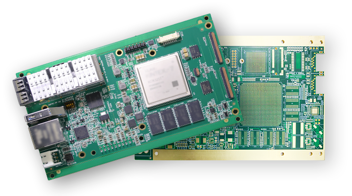
A double sided PCB (two-layer PCB) uses an insulating substrate with copper laminated on both the top and bottom surfaces, with plated-through holes (PTHs) providing electrical connections so signals and power can flow between the two layers. This design allows the board to support surface-mount devices (SMD), through-hole components, or mixed-technology assemblies on the same board. Because both sides are available for routing, engineers gain far greater layout flexibility than with single-sided boards, while the overall cost and manufacturing complexity remain much lower than those of multilayer PCBs.
When designing a double sided PCB, component placement should always follow a logical and thermally efficient layout strategy. High-heat devices should be positioned away from temperature-sensitive components, while analog and digital signal areas should remain physically separated to minimise interference. Pads that carry high current loads should be reinforced to improve long-term reliability, and SMD components must be placed in a way that ensures mechanical stability during reflow and operation. A well-planned placement strategy not only improves circuit performance, but also enhances manufacturability and assembly yield.
In a double sided PCB, vias act as the key interconnection structures between the top and bottom copper layers, so their use should be carefully controlled. Properly placed vias help maintain signal integrity, reduce routing congestion, and keep drilling and plating costs under control. However, excessive via usage may weaken the PCB mechanically and complicate the manufacturing process. Therefore, via density, spacing, and positioning should be optimised to balance routing convenience with structural reliability and production stability.
A double sided PCB offers valuable flexibility for designing efficient power and grounding systems. Designers can allocate wider copper areas for power distribution, establish low-impedance ground networks, and reduce noise by improving current return paths. Implementing solid or partial ground planes is often recommended to stabilise reference potentials and control EMI levels. When grounding and power routing are handled correctly, the board benefits from improved electrical performance, reduced noise, and greater operational stability.
Thermal considerations are critical in double sided PCB design, especially in power-related applications. Factors such as copper thickness, pad spacing, component placement, and heat dissipation paths must be evaluated to prevent localised temperature buildup. High-power devices should be positioned where heat can spread effectively, and thermal relief patterns may be applied to balance solderability and heat flow. Good thermal design improves long-term reliability, protects components from overheating, and extends the overall service life of the PCB.
A double sided PCB offers a practical balance between electrical performance and manufacturing cost. Compared with a single-sided board, it provides far more routing space and layout flexibility. At the same time, it avoids the higher production cost and stack-up complexity of multilayer PCBs. For many consumer, industrial, and power-related products, a double sided PCB delivers the right level of performance without exceeding budget limits.
Because a double sided PCB has copper on both sides, signals, power paths, and grounding structures can be arranged more efficiently. Sensitive signals can be separated from noisy power lines, return paths can be optimized, and trace lengths can be reduced. This improves signal integrity and reduces interference, which is difficult to achieve on a single-layer board.
With a double sided PCB, engineers can combine surface-mount components with through-hole parts in the same design. Small SMD devices can be mounted on one side, while connectors or other mechanically stressed components can be reinforced on the other. This flexibility is especially useful in applications such as power modules, controllers, and compact consumer devices.
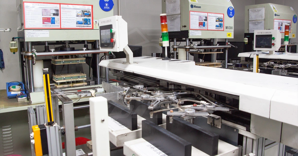
The manufacturing process for a double sided PCB is stable and well-standardized. It does not require complex multilayer lamination, so yields are high and lead times are shorter. This makes production more predictable and easier to scale, which is important for long-term and high-volume product lines.
A double sided PCB helps spread heat more evenly because copper exists on both sides of the substrate. This is valuable in power electronics, LED products, chargers, and motor drivers. Structurally, the two-layer construction also improves board strength, making it more resistant to vibration and mechanical stress.
A double sided PCB significantly increases routing capability compared with a single-layer board, yet remains much more economical than a multilayer PCB. For many mid-complexity designs, it represents the most efficient engineering solution, providing sufficient density, solid electrical performance, and reliable manufacturability at a controlled cost level.
SprintPCB provides reliable double sided PCB manufacturing services for global electronics customers who need stable quality and competitive pricing. Each SprintPCB double sided PCB is produced with copper layers on both sides of the board, allowing components to be mounted on the top and bottom surfaces. This helps engineers achieve higher circuit density and more flexible layouts compared with single-sided designs, making the products suitable for power supplies, LED drivers, consumer electronics and various control systems.
To meet different technical requirements, SprintPCB offers FR-4 standard, high-performance and halogen-free materials, with finished copper thickness from 0.5 oz to 6 oz and board thickness ranging from 0.40 mm to 6.0 mm. Precision capability includes 0.075 mm minimum trace/space and 0.15 mm mechanical drilling, while available surface finishes include HASL, LF-HASL, OSP, ENIG, immersion silver, immersion tin, electrolytic gold and gold fingers. With stable production, responsive technical support and export-ready service, SprintPCB double sided PCB products offer a dependable sourcing option for overseas OEMs and electronics manufacturers.
The double sided PCB plays a vital role in modern electronic engineering by offering more routing capability, component flexibility, and dependable performance than single-sided boards, while remaining far more economical than multilayer PCB structures.
Whether used in power electronics, industrial systems, consumer devices, or automotive modules, a well-designed double sided PCB ensures consistent electrical performance, structural stability, and manufacturing efficiency — making it one of the most practical PCB technologies available today.

Customer support