Printed Electronics Technology is an innovative method that allows electronic functionality to be directly printed onto a substrate. It utilizes specialized printing equipment and conductive inks to create circuits and components on the substrate through a process similar to traditional printing. This approach simplifies the manufacturing process, reduces assembly steps, and enhances production efficiency. Compared to traditional manufacturing processes for electronic components and products, which are characterized by complex procedures, significant material waste, high equipment investments, and environmental pollution, printed electronics technology emerges as an ideal solution due to its simple production processes and lower material consumption. It enables large-area, lightweight, flexible, and cost-effective manufacturing. Furthermore, as a room-temperature printing process, printed electronics can significantly reduce energy consumption and allow for the use of flexible materials such as low-cost plastic films, paper, and fabric as substrates, even with lower heat resistance. As a green manufacturing technology, it also addresses the issues associated with chemical etching processes and the discharge of waste liquids. By adopting organic functional materials and substrates with excellent biodegradability, it fundamentally tackles the problem of environmental pollution caused by electronic products. Therefore, printed electronics technology is widely regarded as a revolutionary solution for the development of the electronics industry. One of the key technological aspects in printed electronics is the use of conductive inks. Conductive inks are typically functional inks that exhibit conductivity. There are two main types of conductive inks: intrinsic conductive inks, which utilize conductive polymers, and doped conductive inks, which incorporate conductive particles. The composition of doped conductive inks includes conductive fillers, binders, solvents, and additives. The selection of conductive fillers depends on the specific requirements of the final product and can involve various types of particles with different conductivity capabilities and characteristics, such as metal-based particles, carbon-based materials, and metal oxide particles. The processing and formulation of these particles often involve the development of nanotechnology, for instance, in the case of the metal-based conductive pastes we primarily employ, which utilize nano-silver-coated copper particles as the conductive filler and are processed using various nanomaterial fabrication techniques. In the development of printed electronics, the innovation and optimization of conductive inks play a crucial role. They not only provide reliable conductivity but also consider requirements such as compatibility, adhesion, and stability with substrates. With the continuous advancement of printed electronics technology, the research, development, and application of conductive inks will bring more opportunities and breakthroughs to the electronics manufacturing industry.
The application of 3D printing technology in PCB manufacturing is rapidly advancing. Originating in the 1980s, it has become a reality with the advancement of 3D printing techniques. This method allows for the direct printing of circuits and components in three-dimensional space, offering increased degrees of freedom and design flexibility. 3D printing technology, also known as additive manufacturing, enables the manufacturing process by constructing physical objects layer by layer. With dedicated 3D printing equipment and materials, digital models can be transformed into tangible physical products. Compared to traditional methods of direct processing and cutting, three-dimensional printing technology has brought disruptive changes to the field of electronic manufacturing. Firstly, 3D printing technology simplifies the manufacturing process. Traditional manufacturing processes involve complex machining steps and tools, while 3D printing technology directly transforms digital design files into tangible physical products, eliminating the need for cumbersome process adjustments and manufacturing preparation time. This significantly shortens the product development cycle and improves production efficiency. Secondly, 3D printing technology offers a high degree of design freedom. It enables highly customized production by creating complex structures and shapes based on specific requirements. Traditional manufacturing methods are constrained by machine tools and process limitations, whereas 3D printing technology can overcome these restrictions, providing designers with a greater creative space. In addition, 3D printing technology enables precise material utilization and minimization of waste. Traditional manufacturing methods often require a significant amount of material for processing and cutting, whereas 3D printing technology allows for precise material usage based on design requirements, thereby reducing material waste and costs. Most importantly, 3D printing technology provides a platform for innovation and rapid prototyping. It enables rapid design iterations, allowing designers to quickly validate and improve designs by printing multiple versions of prototypes. This is crucial for the development and optimization process of electronic products. In general, additive manufacturing, also known as 3D printing, has revolutionized the traditional methods of electronic manufacturing by offering streamlined manufacturing processes, highly customizable designs, precise material utilization, and the advantages of innovation and rapid prototyping. It has introduced a new manufacturing paradigm to the electronics industry, enhancing the speed of product development and unlocking new possibilities for innovation.

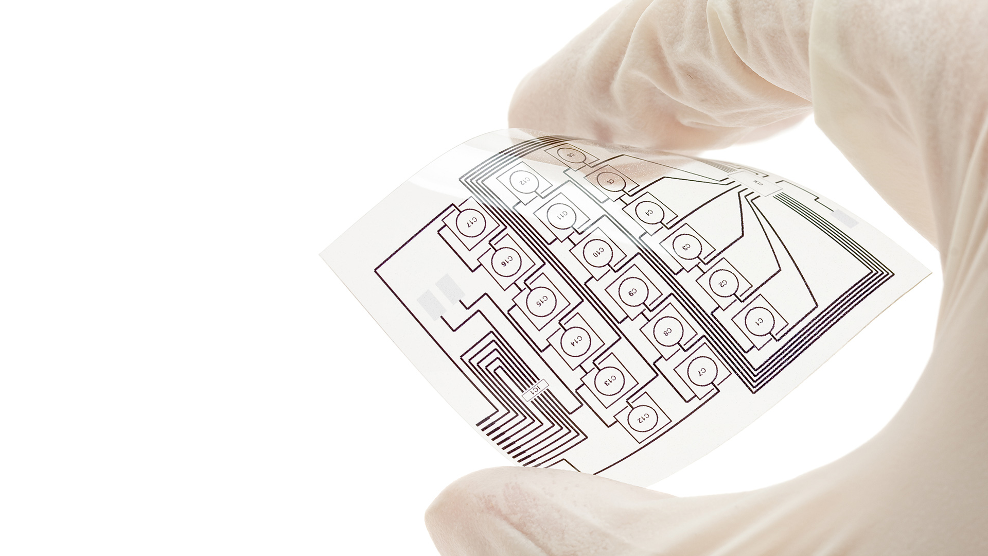
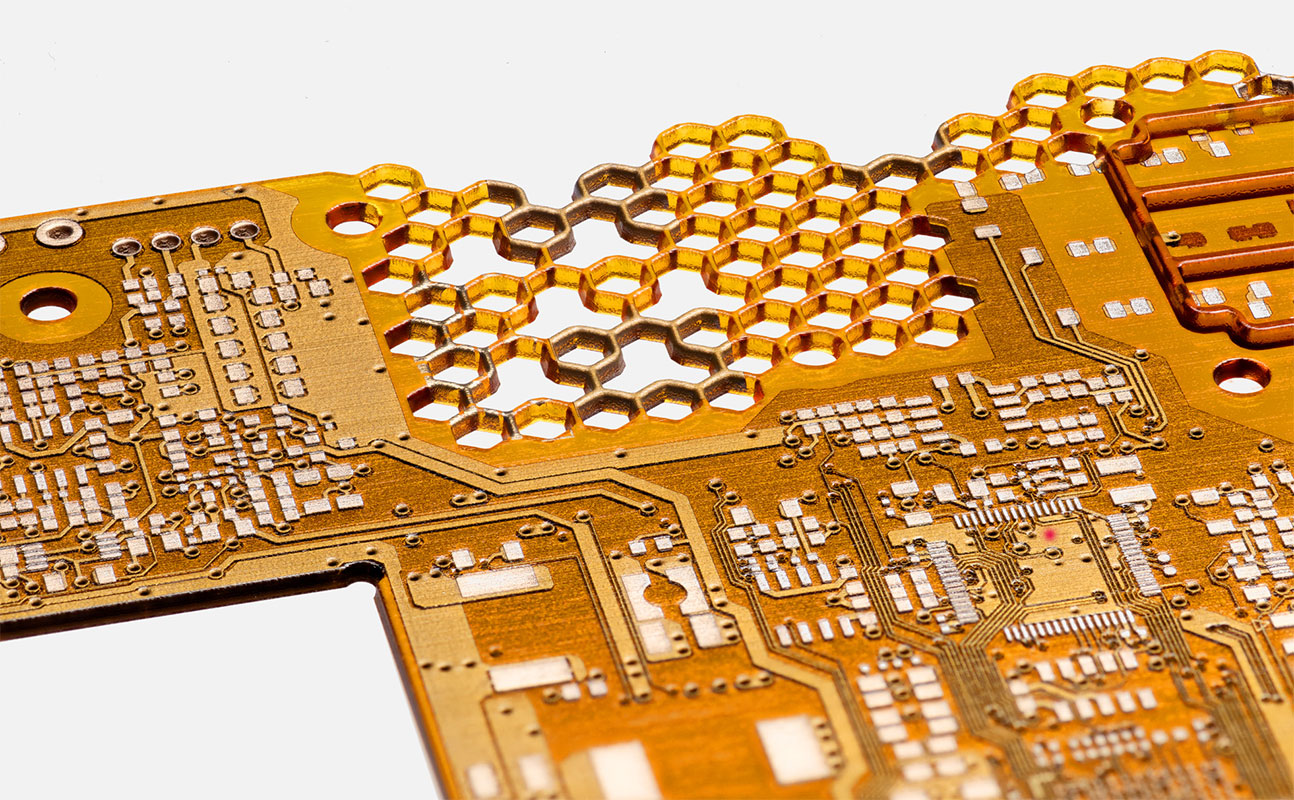
Flexible electronics technology originated in the 1990s and has been widely promoted with advancements in flexible materials and manufacturing processes. It involves manufacturing electronic components on flexible substrates, enabling them to have bending and stretchability. This approach has revolutionized the form and applications of PCBs, creating new opportunities for innovation. Flexible electronics technology is an innovative manufacturing method that provides electronic products with flexibility, bendability, and thinness. Compared to traditional rigid electronic devices, flexible electronics technology offers numerous unique advantages and application prospects. Firstly, flexible electronics technology enables electronic devices to function normally even when bent, curved, or deformed. This makes them suitable for various applications that require adaptation to complex shapes or surfaces, such as wearable devices, smart garments, flexible displays, and more. By utilizing flexible substrates and components, flexible electronic products exhibit excellent mechanical resilience and adaptability. Secondly, flexible electronics technology offers the advantage of being lightweight and compact. Compared to traditional rigid electronic products, flexible electronic products excel in terms of weight and size. This makes them highly suitable for a wide range of applications in fields such as aerospace, automotive, healthcare, and mobile devices. The lightweight design of flexible electronics enables enhanced portability and flexibility for the products. Additionally, flexible electronics technology offers advantages in scalability and high production efficiency. By utilizing efficient manufacturing methods such as printing, coating, and laser processing, large-scale and low-cost production of flexible electronic products can be achieved. Compared to traditional rigid electronics manufacturing methods, flexible electronics technology can reduce material waste and process complexity, thereby improving production efficiency and reducing costs. Most significantly, flexible electronics technology provides a tremendous opportunity for innovation and multifunctionality. Through the integration of flexible substrates and advanced electronic components, various functionalities can be achieved, including bendable sensors, rollable batteries, and flexible circuits. This opens up vast opportunities for exploring new applications and markets, ranging from smart healthcare to intelligent transportation, as well as the Internet of Things (IoT) and wearable technologies. In general, flexible electronics technology represents a significant breakthrough in the field of electronic manufacturing. It not only endows electronic products with flexible and bendable characteristics but also offers advantages in terms of lightweight, scalability, and efficient production. With further technological advancements, flexible electronics technology will bring forth even more innovation and transformation across various domains.
Nanoprinting technology originated in the early 21st century and has been further refined with the development of nanoscale precision manufacturing techniques. This method utilizes nanoscale precision printing techniques to fabricate tiny circuits and structures on PCBs, providing support for miniaturized and high-performance electronic devices. Nanoprinting technology is a revolutionary manufacturing method that leverages nanoscale precision control to achieve fine processing and assembly of materials. It directly prints patterns or structures on substrates at the nanoscale level, opening up new possibilities for various applications in different fields. Firstly, nanoscale printing technology offers advantages of high precision and high resolution. By utilizing nanoscale printing heads and precise control systems, it can achieve accurate replication of tiny sizes and complex structures on substrates. This makes nanoscale printing technology widely applicable in fields such as optoelectronics, microelectronics, biomedicine, and sensors. It provides an effective manufacturing method for producing high-resolution displays, microcircuits, nanosensors, and other products. Secondly, nanoscale printing technology features high efficiency and scalability. Compared to traditional manufacturing methods, nanoscale printing technology enables large-scale, rapid, and cost-effective production. It employs high-speed printing processes and advanced material delivery systems, allowing for fast nanoscale pattern replication and manufacturing. This positions nanoscale printing technology with great potential for industrial production and large-scale manufacturing, offering new pathways for efficient and low-cost production of nanodevices. Additionally, nanoscale printing technology offers advantages of multifunctionality and material diversity. By selecting different printing materials and nanoscale pattern designs, it enables the fabrication of various functional structures and materials. For example, it can use nanoscale metal particles to create conductive patterns or employ nanoscale particles or fibers to produce filters or biosensors. Nanoscale printing technology provides flexibility and innovation in designing and manufacturing nanodevices with multiple functions and characteristics. Lastly, nanoscale printing technology provides robust support for research and applications in the fields of nanoscience and nanotechnology. It offers a controlled and cost-effective approach for the fabrication of nanomaterials, nanostructures, and nanodevices. The development of nanoscale printing technology serves as a powerful tool for the promotion and commercialization of nanotechnology, fostering further advancements and applications in nanoscience. In conclusion, nanoscale printing technology is an advanced manufacturing method with advantages such as high precision, high efficiency, multifunctionality, and material diversity. It holds extensive prospects for applications across various fields, driving innovation and breakthroughs.
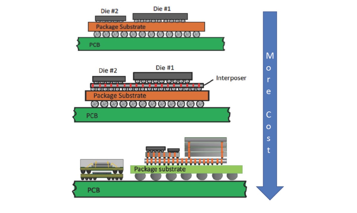
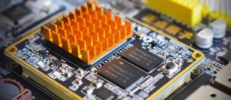
Stacked packaging technology originated in the 1990s and has evolved with advancements in chip packaging and stacking techniques. This approach involves stacking multiple packaging layers within a single chip, enabling higher levels of integration and performance. Stacked packaging technology is an advanced integrated circuit packaging method that involves vertically stacking multiple chips or modules on a single die, enabling higher levels of integration and performance. This technique finds widespread application in high-performance computing, mobile communications, artificial intelligence, and cloud computing, among other fields, delivering significant enhancements to the functionality and performance of electronic devices. The key to stacked packaging technology lies in stacking multiple chips or modules together and interconnecting them through micro-sized interconnects. This stacking structure enables a more compact package size and shorter signal transmission paths, thereby enhancing circuit speed and responsiveness. Additionally, by stacking chips vertically, space utilization is maximized, leading to higher integration and functional density. There are two main approaches to implementing stacked packaging technology: silicon interposers and chip-to-chip bonding. Silicon interposers involve stacking multiple functional modules on the same chip, enabling interconnection and packaging through wafer-level packaging processes. This approach reduces the number of external package pins, thereby improving circuit performance and reliability. Chip-to-chip bonding, on the other hand, refers to the stacking of different chips or modules together and connecting them through fine interconnects. This approach enables high-speed communication and data exchange between chips with different functionalities. Stacked packaging technology offers several advantages. Firstly, it provides higher integration and functionality density, allowing devices to incorporate more features within limited space. Secondly, stacked packaging technology enables shorter signal transmission paths, reducing signal delays and improving circuit response speed.
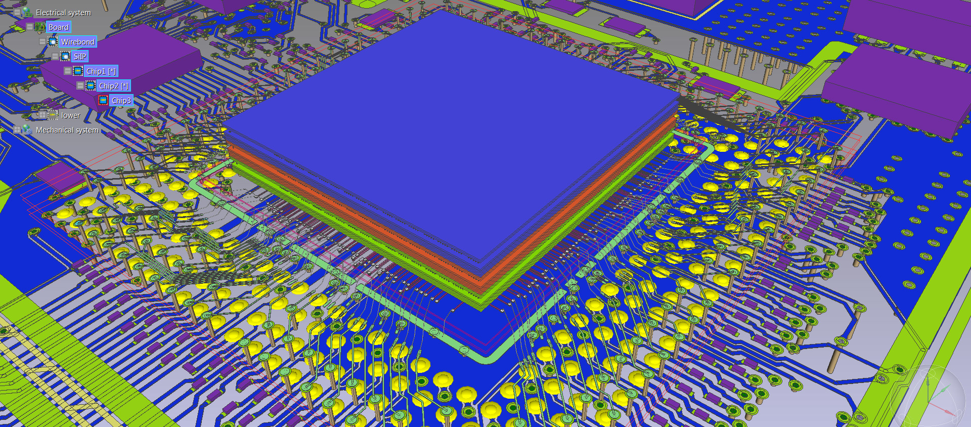
Additionally, by utilizing stacked packaging, different functional chips or modules can be integrated together, reducing system volume and power consumption. Lastly, stacked packaging technology also enhances heat dissipation performance, enabling more effective cooling of high-power chips and improving system stability and reliability. In summary, stacked packaging technology is a disruptive innovation that brings significant advancements to integrated circuit packaging and performance. By stacking multiple chips or modules, it enables higher integration, faster speeds, and smaller form factors, thus driving the development and innovation of electronic devices.
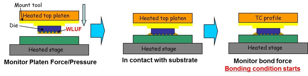
Thermocompression bonding technology originated in the 1990s and has been widely adopted with advancements in packaging and bonding techniques. It involves using heat and pressure to establish a reliable connection between the chip and the substrate, resulting in superior electrical performance. Thermocompression bonding technology is an innovative bonding method widely employed in the field of electronic manufacturing. It achieves reliable connections between wires and the surfaces of electronic devices through high-temperature and high-pressure conditions. The process of thermocompression bonding requires precision and specialized equipment and processes. Firstly, the wires are closely brought into contact with the metal surfaces of electronic devices and subjected to high temperatures and pressures. The high temperature renders the metal surfaces malleable, while the high pressure induces metal diffusion, resulting in a robust metal bond. Through this method, a reliable electrical connection is established between the wires and electronic devices. The thermocompression bonding technique offers several advantages. Firstly, it provides excellent electrical performance and connection reliability. Due to the high strength of the metal bonding, the resistance and voltage drop in the bonding region are low, ensuring good signal transmission and electrical performance. Additionally, the high temperature and pressure during the bonding process help remove oxide layers and contaminants, ensuring the quality and reliability of the connection. Secondly, thermocompression bonding is suitable for a variety of materials and components. It can be used to connect metal wires to semiconductor devices, chips, electronic packaging, and substrates, among other material combinations. This flexibility makes thermocompression bonding a crucial process in electronic manufacturing. Furthermore, thermocompression bonding offers efficiency and automation advantages. It can achieve multiple bonding connections in a short period, making it suitable for large-scale production. Moreover, with the application of automated equipment, the bonding process can achieve high precision and consistency, improving production efficiency and product quality. In summary, thermocompression bonding is an important electronic interconnection method that offers excellent electrical performance, connection reliability, and applicability. It plays a critical role in electronic manufacturing, providing a reliable connection solution for various electronic devices' manufacturing and assembly.
The application of photolithography technology in PCB manufacturing has been continuously advancing. It originated in the 1960s and has evolved with the progress of photolithography equipment and materials. New photolithography techniques have made it possible to achieve smaller line widths and higher resolutions, thereby improving the density and performance of circuit boards. Photolithography technology is a crucial process step in integrated circuit manufacturing. It involves transferring patterned designs onto a photoresist layer using photoresist and photomasks, thereby forming the desired patterns on the surface of the chip. With the constant advancement of technology, photolithography has undergone numerous innovations and advancements to meet the increasingly complex and precise requirements of integrated circuit manufacturing. Firstly, resolution is one of the key directions in the development of lithography technology. As chip sizes shrink and device density increases, manufacturing precision and pattern resolution become crucial. To achieve higher resolution, using shorter wavelengths is a key strategy. From ultraviolet (UV) to deep ultraviolet (DUV) and extreme ultraviolet (EUV), lithography technology has gradually adopted shorter wavelengths to improve resolution and achieve smaller device sizes and higher integration. Secondly, the resist material in lithography technology is also constantly innovating. The resist is a critical image transfer medium, and its performance directly affects the accuracy and quality of pattern transfer. To meet higher resolution and more complex process requirements, new generations of resistant materials continue to emerge. For example, the introduction of chemical amplified resist (CAR) and anti-reflective coating (ARC) technologies has improved the resolution, contrast, and optical performance of the resist, resulting in better pattern transfer effects. In addition, lithography technology has made significant progress in multi-layer and multi-mode processing. To achieve more complex chip designs and functionalities, multi-layer lithography steps and precise overlay of different pattern modes are required. The introduction of multiple patterning techniques, multi-mode lithography, and dual anti-reflective coating (DARC) methods provides lithography processes with higher flexibility and precision, enabling the manufacturing of complex chip structures. Finally, lithography technology also faces challenges and directions for development. For example, emerging technologies such as self-aligned lithography (SAL) and electron beam lithography (EBL) have been proposed and researched to meet the demands for smaller sizes and higher resolution compared to traditional lithography techniques. These technologies offer potential solutions through different principles and methods to achieve finer pattern transfer and higher manufacturing efficiency. In conclusion, lithography technology plays a critical role in integrated circuit manufacturing and is continuously undergoing innovation and development. By continuously improving resolution, enhancing resist materials, implementing multi-layer and multi-mode processes, and exploring new lithography technologies, we can expect further breakthroughs in lithography technology in the future, bringing higher accuracy, greater flexibility, and better performance to integrated circuit manufacturing.

Data-driven manufacturing utilizes technologies such as big data, artificial intelligence, and machine learning to optimize the PCB manufacturing process. It originated in the early 21st century and has been widely promoted with the development of data analytics and intelligent algorithms. Through real-time data analysis and intelligent algorithms, the manufacturing process can be monitored and optimized more accurately and efficiently, thereby improving production efficiency and quality. Data-driven manufacturing is a manufacturing approach based on big data and advanced analytics techniques. It involves collecting, analyzing, and applying data to optimize production processes and decision-making, thereby enhancing production efficiency, quality, and flexibility. First, data-driven manufacturing relies on real-time data collection and monitoring. Key parameters and indicators in the manufacturing process can be recorded and monitored in real time through sensors, IoT devices, and other data collection technologies. These data can cover various aspects from raw materials to finished products, including supply chain, production equipment status, process parameters, product quality, and more. First, data-driven manufacturing relies on real-time data collection and monitoring. Key parameters and indicators in the manufacturing process can be recorded and monitored in real time through sensors, IoT devices, and other data collection technologies. This data can cover various aspects from raw materials to finished products, including supply chain, production equipment status, process parameters, product quality, and more. Based on the results of these data analyses, manufacturing companies can take real-time control and adjustment measures to optimize the production process. For example, by monitoring equipment status in real time and predicting maintenance needs, sudden failures and downtime can be reduced. By monitoring production parameters and quality indicators in real time, process parameters can be adjusted, and product quality can be improved. Furthermore, data-driven manufacturing can support intelligent decision-making and planning. By applying big data and advanced analytics to supply chain management, demand forecasting, and production planning, manufacturing companies can achieve more accurate demand prediction, more efficient inventory management, and optimized production planning. This helps reduce inventory costs, improve delivery capabilities, and meet customer demands. Overall, data-driven manufacturing is a method that utilizes data and analytics technologies to optimize the manufacturing process and decision-making. It can help manufacturing companies achieve more efficient, flexible, and quality production, thereby improving competitiveness and customer satisfaction. With the continuous development of technology and the accumulation of data, data-driven manufacturing will play an increasingly important role in the manufacturing industry. These innovative PCB manufacturing methods originated in different periods, and with the advancement of technology and the widespread adoption of applications, they have brought us numerous potential benefits. From improving production efficiency to expanding design space, from enhancing performance to achieving higher reliability, these methods have provided groundbreaking advantages to the field of PCB manufacturing. It is crucial for us to seize these opportunities and continuously explore and implement innovative manufacturing methods to drive the development and innovation of the electronics industry.

Customer support