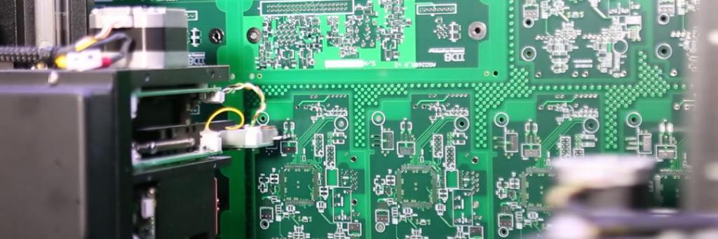
Impedance control, in simple terms, ensures that electrical signals travel smoothly along a printed circuit board (PCB) without distortion or reflection—much like keeping a highway's lanes uniform and the surface even, so cars run steadily without bumping or swerving. For high-speed and high-frequency applications such as 5G communications, AI servers, automotive electronics, and medical devices, precise impedance control is crucial to guarantee signal integrity and reliability.

Single-ended impedance: Single-ended impedance refers to the impedance of a single signal trace relative to a reference plane (usually ground or power). It is commonly found in digital circuits and clock signal transmission.
Differential impedance: Differential impedance is formed by a pair of traces carrying complementary signals (positive and negative). This configuration provides strong noise immunity and reduces electromagnetic radiation, making it ideal for USB, HDMI, LVDS, PCIe, and 5G communication interfaces. Differential impedance control is more complex than single-ended, as it depends not only on trace width and dielectric thickness, but also on trace spacing, parallelism, and manufacturing consistency.
Coplanar waveguide impedance and microstrip/stripline impedance: Coplanar waveguides are often used in RF circuits; the signal line is flanked by ground planes to better control electromagnetic field distribution. Microstrip lines are located on the PCB surface, with both air and dielectric as the medium. Striplines, embedded between two reference planes, are better suited for high-speed, high-integrity signal transmission.
The dielectric constant (Dk) and dissipation factor (Df) of materials directly influence signal propagation speed and attenuation. Standard FR4 suits most multilayer PCBs. For high-frequency, high-speed applications, materials like Rogers and Megtron offer more stable Dk and lower Df. SprintPCB selects materials based on customer requirements and application environments to ensure reliable impedance characteristics from the ground up.
Impedance is highly sensitive to trace geometry—even a few micrometers of variation can cause deviations from design targets. Therefore, trace width and spacing must be tightly controlled during manufacturing, demanding extremely stable etching processes. Over-etching or under-etching can alter trace width, impacting impedance. SprintPCB employs high-precision LDI laser exposure and automated etching systems to maintain minimal variation, ensuring impedance consistency.

During lamination, any variation in dielectric thickness—caused by temperature or pressure curve deviations—can shift impedance values. SprintPCB utilizes precise lamination curve control to ensure uniform dielectric thickness across layers, achieving stable impedance even in volume production.
Copper thickness and surface finish also influence impedance. For instance, 35 μm and 18 μm copper layers produce significantly different impedance values. Surface finishes such as ENIG or electroplating slightly alter surface morphology, subtly affecting signal transmission. SprintPCB rigorously controls plating and finishing processes and validates results using TDR (Time Domain Reflectometry) testing to ensure measured impedance matches design targets.

Differential signaling is a widely adopted impedance control method. By transmitting signals through a positive/negative pair, noise resistance is enhanced and EMI is reduced. SprintPCB ensures differential impedance consistency by precisely controlling trace spacing, width, and dielectric thickness.
Accurate trace width and spacing are essential for target impedance. Designers must consider dielectric constant, copper thickness, and reference planes, using impedance calculators or simulation tools. Consistent geometry reduces crosstalk and preserves signal integrity. SprintPCB's LDI exposure and automated etching guarantee faithful reproduction of design parameters for repeatable impedance control.
Ground and reference planes play a vital role in impedance stability. The ground plane provides a signal return path, keeping impedance constant. The reference plane establishes a uniform potential baseline, aiding signal integrity. Through optimized stack-up design and controlled layer spacing, impedance can be effectively managed across the PCB.
Reducing impedance often involves adjusting material properties and trace geometry. Lower Dk materials speed up signal propagation and reduce impedance. Adjusting trace width and copper thickness fine-tunes impedance. As copper thickness increases, inductance decreases and capacitance increases, resulting in lower impedance—thus, careful copper control is crucial.
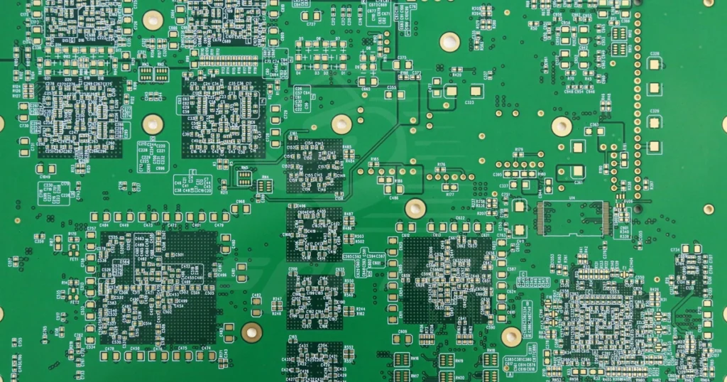
In SprintPCB's production, the engineering team develops precise stack-up models based on customer impedance targets, optimizing trace width, spacing, and layer configurations. During production, lamination is tightly managed using imported high-flatness presses and steel plates, achieving flatness within 0.02 mm/m² and dielectric thickness tolerance within 5%. Acid etching delivers smooth sidewalls with an etching factor of 4–6, minimizing dimensional variation. High-precision TDR testing ensures final impedance values remain within tight tolerance ranges, guaranteeing reliable, repeatable performance across batches.

Customer support