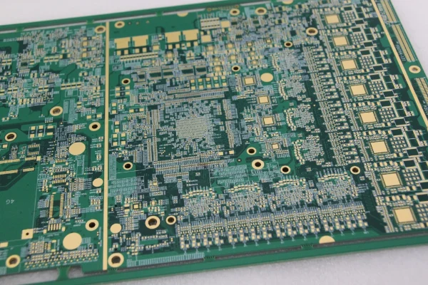
As electronic products continue to become smaller, faster, and more powerful, designers and manufacturers face increasing pressure to achieve higher functionality within limited space. Traditional PCB technologies often struggle to meet the requirements of modern compact electronics, especially when signal integrity, miniaturization, and reliability are critical. This is where HDI multilayer PCB technology becomes essential. By enabling ultra-fine circuit routing, microvias, and advanced layer stacking, HDI multilayer PCBs offer a proven solution for high-density interconnection challenges in today's electronics. This article provides a comprehensive, user-focused explanation of HDI multilayer PCB technology, how it solves real engineering problems, and why it is widely used in compact, high-performance electronic devices. It also introduces SprintPCB HDI multilayer PCB manufacturing capabilities as a practical reference for implementation.

An HDI multilayer PCB (High-Density Interconnect multilayer printed circuit board) is a type of advanced PCB designed to support significantly higher wiring density per unit area compared to conventional multilayer boards. This increased density is achieved through the use of microvias, blind vias, buried vias, fine line widths, and tighter spacing.
Unlike traditional PCBs that rely primarily on mechanically drilled through-holes, HDI multilayer PCBs utilize laser-drilled micro blind vias and buried vias, allowing designers to route signals more efficiently between layers while minimizing board size.
HDI multilayer PCB structures commonly range from 1+N+1 to 4+N+4, where “N” represents the core layers and the additional layers are sequentially built up using advanced lamination techniques. This structure provides exceptional flexibility for high-speed, high-density designs.
Compact electronic products leave very little room for traditional PCB routing. As product dimensions shrink, designers cannot simply increase board size or thickness to accommodate more circuitry. An HDI multilayer PCB maximizes available space by allowing routing to occur vertically through microvias instead of horizontally across large surface areas. This vertical interconnection capability enables more efficient use of every square millimeter of the board.
As a result, designers can integrate more functions into a smaller footprint, which is essential for today's slim, lightweight electronic devices.
Modern IC packages such as fine-pitch BGAs, CSPs, and system-in-package solutions require extremely dense routing around component pads. Traditional PCB technology often struggles to fan out these components without increasing layer count or compromising signal quality.
HDI multilayer PCB technology supports fine trace widths and tight spacing, allowing engineers to route signals cleanly and efficiently from dense component layouts. This reduces routing congestion and improves overall design reliability.
In addition to space and routing density, modern electronics place strict requirements on overall board thickness and weight. Portable and wearable devices, in particular, demand thinner and lighter PCBs without sacrificing functionality.
An HDI multilayer PCB enables thinner board designs by replacing large mechanical through-holes with compact microvias. Because microvias occupy less vertical space, designers can reduce overall board thickness while still increasing the number of functional layers. This makes it possible to build higher-layer-count PCBs within a compact profile, supporting complex signal routing, power distribution, and grounding strategies in a limited space. The result is a lighter, thinner PCB that still delivers high performance and structural reliability.
HDI multilayer PCB technology therefore plays a critical role in products where mechanical constraints and electrical complexity must be balanced simultaneously.
In high-speed digital and RF designs, signal integrity is directly affected by trace length, impedance discontinuities, and parasitic effects. HDI multilayer PCB technology significantly shortens interconnection distances by allowing signals to transition between layers using microvias placed close to component pads.
By shortening interconnection distances, HDI multilayer PCBs reduce signal loss, reflection, and timing skew, resulting in cleaner and more stable signal transmission.
Traditional vias and wide traces can introduce parasitic capacitance and inductance that negatively affect high-frequency signals. HDI multilayer PCBs, with their smaller vias and finer routing, inherently reduce these parasitic effects. This makes HDI multilayer PCB technology particularly suitable for applications requiring stable high-speed data transmission and precise impedance control.
SprintPCB provides professional HDI multilayer PCB solutions tailored for compact, high-performance electronic products. With advanced HDI fabrication technologies and stable process control, SprintPCB supports customers seamlessly from prototype development to mass production, ensuring consistent quality and reliable performance at every stage.
Key HDI PCB capabilities include:
Laser-drilled micro blind vias and buried vias for ultra-fine interconnections
Higher functional density and maximum space utilization for compact designs
Enhanced signal integrity through shorter interconnection paths
Thinner and lighter PCB structures with increased layer counts
Broad application support, including smartphones, tablets, wearable electronics, and other high-density devices
SprintPCB specializes in HDI multilayer PCBs with fine line and spacing, advanced sequential lamination, and high-reliability microvia structures, supporting stack-ups from 1+N+1 to 4+N+4. Through consistent engineering control and manufacturing expertise, SprintPCB helps customers maintain design consistency, improve yield, and reduce project risk throughout the entire product lifecycle.
The HDI multilayer PCB has become an essential technology for modern electronic design, enabling high-density routing, improved signal integrity, and compact form factors.
By leveraging microvias, advanced stack-up structures, and precision manufacturing, HDI multilayer PCBs provide a reliable solution for today's space-constrained, high-speed electronic products. With experienced manufacturers such as SprintPCB offering comprehensive HDI multilayer PCB solutions, designers and buyers can confidently bring complex products from concept to mass production.

Customer support