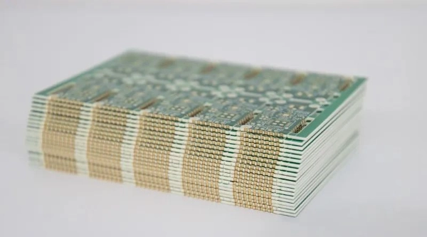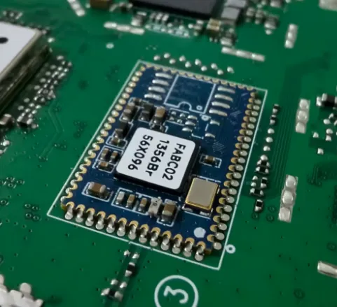
A metallized half-hole is created by drilling a through-hole in a PCB, followed by copper plating and electroplating to form a conductive copper layer. Then, half of the hole is mechanically removed, leaving one half of the hole to serve an electrical function. Unlike a full through-hole, a half-hole has one part located at the board's outer edge, and the other half extends inward. This design is typically used for modular circuit connections and assembly.

Space-saving and Improved Integration: Without the need for additional connectors, direct board-to-board interconnection enables more compact layout designs. It is especially useful in modular circuit assembly, particularly in space-constrained industrial equipment.
Enhanced Mechanical Strength: Traditional pin or header connections are prone to loosening from vibrations or pressure, whereas the half-hole is directly soldered to the edge of the main PCB, creating a secure mechanical bond.
Efficient Modular Interconnection: Half-holes allow various functional circuit modules to be assembled onto the main control board like "building blocks," facilitating both easy disassembly and upgrades, as well as maintenance.
Cost and Process Reduction: The absence of extra connectors and pins simplifies the assembly process. In mass production, it leads to higher yield rates, fewer repairs, and thus, reduced overall costs.
The classic application of metallized half-holes is in modular assembly. For instance, in Industrial Internet of Things (IIoT) devices, sensor modules often need to securely connect with the main control board. The metallized half-hole design allows these smaller modules to be soldered directly onto the main board, saving space and ensuring reliable signal and power transmission.
In automotive control systems, in-vehicle communication modules (such as CAN bus expansion modules) are often connected to the main control unit using a half-hole method, reducing the risk of poor contact from traditional connectors.
Advantages: Seamless connection, compact design, cost reduction.
Industry Applications: Industrial automation, automotive electronics, smart city sensor networks.
Distribution boards are used to route complex chip pins to facilitate easier connection and debugging by developers.
In RF module development, metallized half-hole PCBs are often used to transition high-density chip interfaces to standard pin headers or female headers, enabling engineers to easily conduct testing or integration.
In embedded system R&D, half-hole distribution boards allow design engineers to quickly build verification environments without needing to redesign entire large boards.
Advantages: Simpler assembly, reusability.
Industry Applications: Embedded system development, communication module development, sensor interface boards.
Metallized half-holes can serve as a reliable edge connection method. In rail transportation and power electronics, control modules must withstand high vibration and temperature environments. Compared to plug-in connectors, half-holes directly soldered to the main board offer superior mechanical impact resistance and long-term stability.
In automotive ADAS (Advanced Driver Assistance Systems) modules, half-holes used as edge interfaces optimize space utilization while maintaining signal integrity.
Advantages: Stable connections, space-saving.
Industry Applications: Automotive electronics, railway signal control, industrial control equipment.
Another significant characteristic of metallized half-holes is optimizing space utilization. In aerospace electronics, both reliability and space efficiency are crucial. By using half-hole technology, the number of connectors can be reduced, enhancing vibration resistance, while also saving weight and space.
Advantages: Elimination of redundant connectors, improved compactness.
Industry Applications: Medical electronics, aerospace, industrial sensors.
Metallized half-holes are not just a process structure; they act as a "bridge" that ensures stable and efficient electrical and mechanical connections between modules.
Manufacturing metallized half-hole PCBs is not simple, with common challenges including:
Copper Burrs: After cutting the half-hole, tiny copper burrs may remain, affecting soldering quality.
Residue on Hole Walls: Milling or drilling may leave impurities or burrs, causing poor soldering.
Copper Layer Peeling: Thin boards may experience cutting forces that cause the plating layer to tear, reducing reliability.
Uneven Electroplating: The unique position of the half-hole may lead to uneven distribution of electroplating solution, causing inconsistent copper layer thickness.
If these issues are not addressed properly, they can result in poor soldering and electrical failure.
SprintPCB has industry-leading experience and systematic processes in manufacturing metallized half-holes:
Provides Design for Manufacturability (DFM) suggestions, optimizing hole size, hole spacing, solder ring width, and edge safety distance to prevent design defects and minimize production risks and costs.
Recommends maintaining a minimum finished hole diameter ≥0.4 mm (with a limit of 0.35 mm), hole spacing ≥0.5 mm (compensated to ≥0.4 mm), and solder ring width ≥0.2 mm (with a limit of 0.15 mm). Edge corner distance should be ≥1 mm to ensure copper layer attachment strength and resistance to processing damage.
Employs standardized processes for drilling, copper plating, circuit making, graphic electroplating, milling half-holes, etching, solder resist, marking, and surface treatment. These processes are tightly coordinated for maximum efficiency.
Chemical copper plating process is well-developed, including deburring, swelling, adhesive removal, catalysis, copper plating, followed by rigorous cleaning and drying procedures to ensure uniform and firm copper layer attachment.
Controls copper plating temperature (approximately 25–35°C), pH (11–13), chemical concentration, and timing to ensure stable and reliable copper plating quality.
Multi-stage Quality Inspection: Uses metallographic microscopy to inspect copper plating quality (≥8.5 grade), X-ray thickness measurement, tape adhesion testing, and microscopic hole wall inspection to ensure that each step meets the required standards.
Metallized half-holes are a critical process design that combines space utilization with electrical connection advantages in high-reliability fields such as industrial control, communications, medical, automotive, and power electronics. Their key benefits are straightforward: saving space, improving modular efficiency, and ensuring strong connections.
By leveraging systematic DFM support, rigorous processes, comprehensive quality inspection, and extensive industry experience, SprintPCB can help customers avoid risks in the design phase and ensure stable quality in the manufacturing phase, providing reliable metallized half-hole PCB solutions for demanding industries.

Customer support