In the era of rapid technological advancement, Printed Circuit Boards (PCBs) play a crucial role. PCBs are vital components in electronic devices as they provide reliable electrical connections and mechanical support for various electronic components. With the advancement of technology, the demand for PCBs has become increasingly higher, leading to the emergence of HDI PCBs. HDI (High-Density Interconnect) PCB, as an important branch of PCB technology, has brought revolutionary changes to the design and manufacturing of electronic devices. In the past, traditional PCB designs used larger-sized boards and employed conventional routing methods. However, with the rapid iteration and miniaturization trends in electronic devices, traditional PCBs fail to meet the growing requirements. People have started to pursue smaller sizes, higher performance, and greater reliability, leading to the demand for HDI PCBs.
HDI PCB, as an advanced technological solution, significantly enhances the performance, reliability, and integration of circuit boards through the utilization of multi-layered thin boards and fine-line circuits. It has found wide-ranging applications across various industries, owing to its unique advantages. In this article, we will delve into what HDI PCB is and unveil its remarkable benefits. Through this article, you will discover HDI PCB and why it has gained such popularity. We will discuss the advantages of HDI PCB over traditional PCBs and showcase its wide-ranging applications in various fields. Additionally, we will explore the key design considerations, manufacturing processes, and future trends of it. Let's now uncover the mysteries of HDI PCB together and discover its untapped potential. The repeated mention of HDI is bound to raise questions:
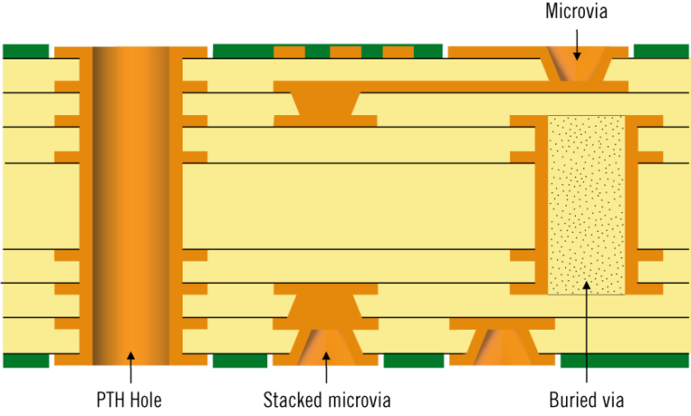
HDI, which stands for High-Density Interconnect, is an advanced PCB (Printed Circuit Board) technology characterized by high circuit density, small size, and high integration. HDI PCB utilizes micro-sized traces, buried vias, and blind vias to enable components on the board to be connected and arranged more closely. By reducing the length of traces and the distance for current transmission, HDI PCB enhances signal transmission speed and reliability. Furthermore, HDI PCB allows for higher pin and circuit density, enabling more functionalities to be integrated into smaller spaces.
HDI PCB (High-Density Interconnect) is widely used in various industries due to its high performance and versatility. Now, I will introduce the specific applications of HDI PCB in different industry sectors. First, in the application of mobile devices, HDI PCBs can meet the compact size and high-performance requirements of devices such as smartphones and tablets. They support high-density wiring of complex internal circuits in mobile phones, including processors, memory, cameras, touchscreens, and wireless communication modules.

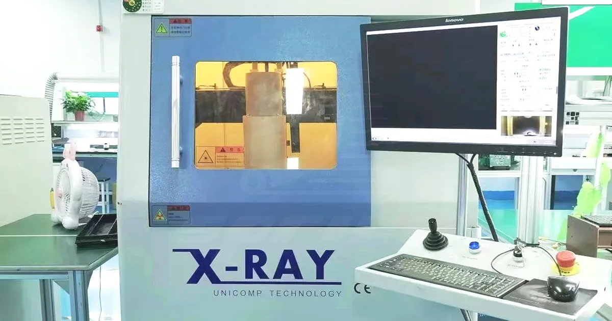
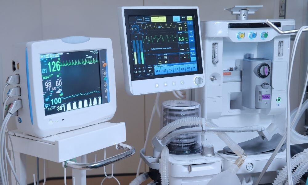
And the small size and lightweight characteristics of HDI PCB make it an ideal choice for wearable devices such as smartwatches, fitness trackers, and smart glasses. Second, the application of communication equipment. HDI PCBS play an important role in communication equipment such as network routers, switches, and modems. They can support high-speed data transmission, complex signal processing, and a variety of connection interfaces. And devices such as wireless base stations, antennas and communication satellites also need high-performance HDI PCBS to meet the needs of signal processing and transmission. Third, the application of medical equipment. HDI PCBS are widely used in medical monitoring equipment and medical imaging equipment, such as electrocardiograph, sphygmomanometer, and glucose meter. They provide accurate signal processing and transmission, supporting accurate monitoring and analysis of medical data. Medical imaging devices such as X-rays, CT scanners and ultrasound devices require high-density circuit boards to process complex image data and signals.
Fourth, on the one hand, HDI PCBS play a key role in automotive audio, video, and navigation systems. They provide high fidelity audio output, high resolution video display, and precise navigation. On the other hand, HDI PCBS are also used in automotive electronic control units, including engine management systems, body control modules and airbag systems. They can support complex signal processing and precise control functions. Fifth, HDI PCBS are widely used in industrial control systems such as factory automation, robot control and sensor networks. They are capable of handling complex control algorithms and high-speed data transmission, providing precise control and monitoring functions. HDI PCBS are also widely used in power distribution systems, energy monitoring equipment, and electronic devices that require high density interconnection to achieve efficient energy conversion and power management. HDI PCB has a wide range of applications. With the continuous progress and innovation of technology, I believe the application of HDI PCB in more fields will continue to expand and deepen.

Customer support