Have you ever wondered how modern electronic products achieve highly complex functionality and performance? In this digital age, smartphones, computers, tablets, and other devices we use heavily rely on advanced electronics manufacturing technology. Among these cutting-edge technologies, Solder Ball plays a seemingly insignificant role, yet it plays a crucially important role.
If you are interested in the electronics manufacturing field, you may have already heard of the term "Solder Ball." So, what is it exactly, and what is its purpose? In this blog post, we will uncover the significance of Solder Ball in the electronics manufacturing industry and its role in chip packaging technology and circuit board connections.
What is a Solder Ball?
First, let's understand what a Solder Ball is.
A Solder Ball is a tiny soldering material, typically composed of tin and other alloy elements. These small balls usually range in diameter from a few tens of micrometers to several hundred micrometers, depending on the specific requirements of the application. Solder Balls can be obtained through specialized manufacturing processes to ensure they have a consistent size and shape, providing the electronics manufacturing industry with a stable and reliable soldering material.
Solder balls are typically made of tin (Sn) as the main component, with the addition of other alloying elements such as lead (Pb), silver (Ag), bismuth (Bi), copper (Cu), etc., to form different soldering alloys. The choice of these alloys depends on the requirements of the application, such as soldering temperature, reliability requirements, and environmental regulations.
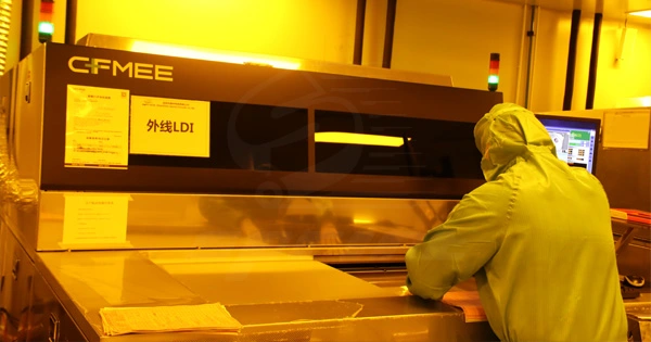
The process of manufacturing Solder Balls
The process of manufacturing Solder Balls requires a high level of precision and control. Common manufacturing methods include:
Sphericalization method:
This method involves dropping liquid metal in a high-temperature environment, forming spherical shapes through surface tension and gravity. It allows the production of larger-scale and more uniformly sized Solder Balls.
Powder metallurgy method:
Solder Ball alloy materials are processed into powder form and then pressed into spherical shapes using specific metallurgical techniques. This method allows for more precise size and composition control.
Gas atomization method:
Alloy materials are heated to a gas atomized state and then formed into Solder Balls through a nozzle spray. This method is suitable for producing small-sized microspheres.
The Role of Solder Ball in Chip Packaging Technology
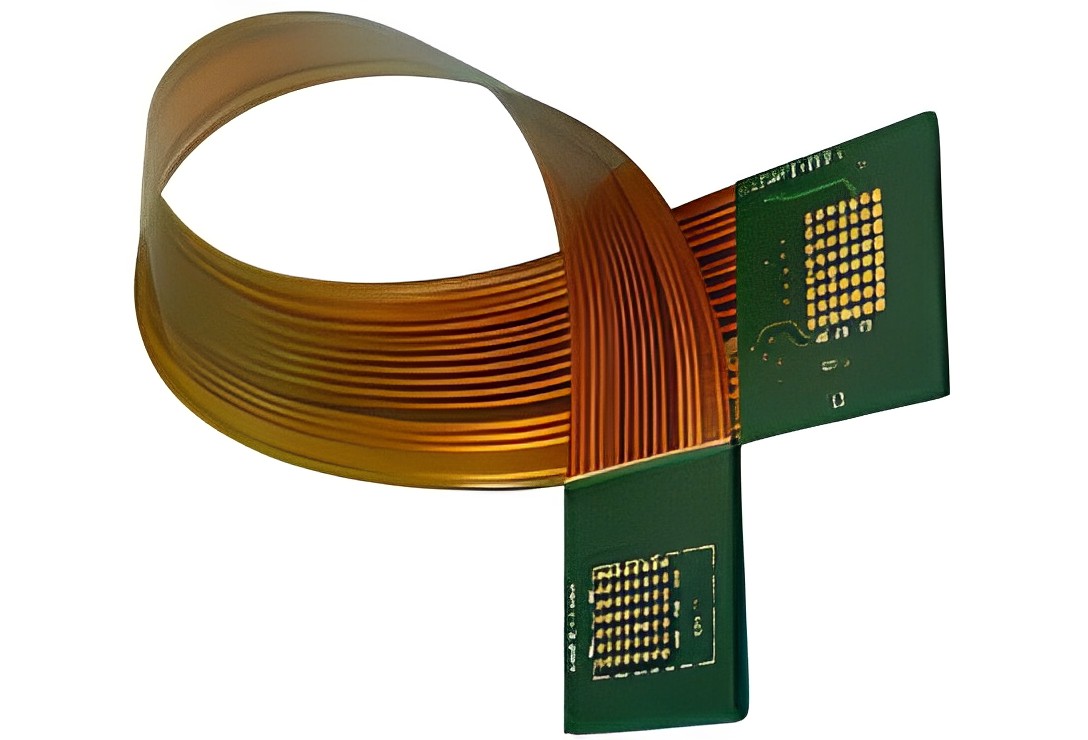
When it comes to circuit board connections, Solder Balls play a crucial role in Surface Mount Technology (SMT). Surface Mount Technology is a method of directly mounting electronic components onto the surface of a Printed Circuit Board (PCB), as opposed to traditional through-hole assembly. Solder Balls act as the bridge between the components and the PCB in Surface Mount Technology, ensuring secure and reliable connections of electronic components on the circuit board.
Surface Mount Technology has become one of the most widely used assembly techniques in modern electronics manufacturing. Compared to traditional through-hole assembly, Surface Mount Technology offers higher component density, shorter manufacturing cycles, and improved performance. In Surface Mount Technology, a layer of solder paste is applied to the solder pads of electronic components, and then the components are accurately placed on these pads. Subsequently, through heating, the Solder Balls in the solder paste melt and form reliable solder connections with the solder pads and the pins of the electronic components.
Solder balls are primarily used in two types of components in Surface Mount Technology:
Surface Mount Devices (SMD)
These components are characterized by their miniaturization, lightweight, and high performance, such as chip resistors, capacitors, transistors, integrated circuits, etc. They typically have exposed solder balls or pads that are connected to the corresponding pads on the PCB through solder ball connections.
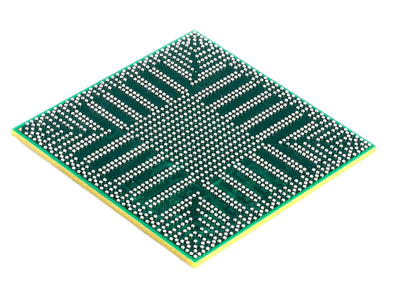
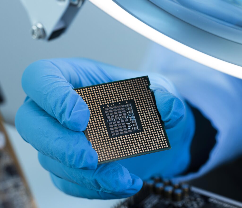
BGA packaging is an advanced chip packaging technology widely used in high-performance and large-scale integrated chips. The bottom of a BGA chip is covered with hundreds or even thousands of tiny solder balls, which are used to connect with corresponding pads on the PCB. The quantity and layout of the solder balls in BGA packaging make it highly popular in high-density packaging.
In the BGA (Ball Grid Array) package, there are many tiny Solder Balls arranged on the bottom of the chip, aligning with the pads on the Printed Circuit Board (PCB). Through processes like reflow soldering, the Solder Balls fuse with the pads to form reliable solder connections, securely attaching the chip to the PCB. The advantages of BGA packaging lie in providing more pin connections, increasing the contact area between electronic components and the PCB, thereby enhancing circuit transmission performance and heat dissipation.
Let's delve into the specific role of Solder Ball in chip packaging technology.
Providing Electrical Connections:
Chips typically have numerous tiny pins that need to be connected to the pads on the circuit board. Solder Balls, as the soldering material, are placed on the bottom of the chip and melted during the manufacturing process to join the chip's pins with the pads on the circuit board. This connection method provides reliable electrical connections, allowing the chip to communicate and function properly with the circuit board.
Mechanical Support Provision:
Chip packaging technology not only requires reliable electrical connections but also demands that the chip is securely fixed on the circuit board during use. Solder balls exist in a spherical form in BGA (Ball Grid Array) packaging, forming a ball-shaped solder joint during the connection process. The design of these ball-shaped solder joints provides mechanical support for the chip, reducing the mechanical stress between the chip and the circuit board. Additionally, it allows for a certain degree of flexibility during temperature changes, thereby enhancing the reliability of the connection.
High-Density Interconnections Support:
BGA (Ball Grid Array) packaging technology allows for a tighter arrangement of chip pins due to the design of its spherical solder balls, enabling high-density interconnections. Compared to traditional soldered pin packages, BGA packaging can provide a greater number of pins, enabling chips to handle more complex functionalities and higher-performance applications. The design and manufacturing of the solder balls determine the pin pitch and count in BGA packaging, making it crucial for achieving high-density interconnections.
Improvement in heat dissipation performance:
In some high-performance and high-power chip applications, heat dissipation is a crucial factor to consider. The presence of solder balls can create tiny gaps between the chip and the circuit board, which play a role in heat dissipation while the chip is in operation. This helps efficiently conduct the heat generated by the chip to the circuit board, thereby enhancing the overall system's heat dissipation performance.
The role of Solder Ball in chip packaging technology is crucial. It not only provides reliable electrical connections and mechanical support but also enables high-density interconnections and improves heat dissipation performance. Through the careful design and manufacturing of Solder Balls, BGA packaging technology achieves higher performance, higher density, and more reliable electronic products. Therefore, in modern electronic manufacturing, optimizing and controlling Solder Balls are essential to ensure excellent performance of electronic products in various application scenarios.
The use of Solder Ball in Surface Mount Technology (SMT) brings some significant advantages and disadvantages compared to traditional through-hole assembly.
Advantages of Solder Ball:
Increased Component Density:
SMT allows more components to be densely installed on the PCB, improving the circuit board's density and performance.
Reduced PCB Size:
Due to the smaller size of SMT components, smaller PCBs can be designed, contributing to lightweight and portability.
Improved Electrical Performance:
Solder Ball provides low resistance and low inductance in soldered connections, benefiting the stability of signal transmission and power supply.
Disadvantages of Solder Balls:
Assembly complexity:
The soldering process involves tiny solder balls, which demand high requirements for equipment and technology during the assembly.
Repair difficulty:
Once the soldering is completed, repairing, or replacing surface-mounted components is more challenging compared to traditional plug-in assembly.
Solder balls play a crucial role in Surface Mount Technology (SMT); they are one of the key components that enable modern electronic products to be compact, high-performance, and high-density. Through reliable connections provided by solder balls, electronic components can be securely mounted on PCBs, forming high-quality solder joints. Despite some challenges associated with Surface Mount Technology, its advantages far outweigh the disadvantages, making it an indispensable technology in the field of electronics manufacturing.
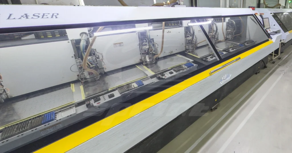
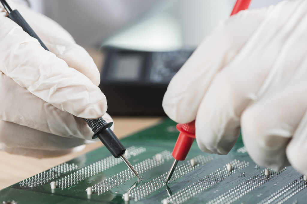
When it comes to ensuring high-quality welding connections, the electronics manufacturing industry must implement a series of process controls, quality inspections, and fault analysis measures.
Firstly, welding process control is a crucial step in ensuring high-quality welding connections. This involves optimizing temperature profiles to ensure that Solder Balls can fully melt and form proper connections with chip pins and solder pads during the welding process. Additionally, regular calibration and maintenance of welding equipment are essential to ensure the accuracy and stability of welding parameters.
Secondly, quality inspection and testing are vital means of verifying the reliability of welding connections. X-ray inspection and ultrasonic testing techniques can non-destructively examine the quality of welding connections, ensuring that there are no voids, cracks, or other defects in the solder joints. Furthermore, subjecting the solder joints to various physical and environmental tests such as impact testing, vibration testing, and temperature cycling testing are critical steps in evaluating welding quality and reliability.
Finally, fault analysis and improvement are an ongoing process to ensure high-quality welding connections. By analyzing common welding faults such as voiding, misalignment, and excessive melting, the root causes of problems can be identified. Based on the results of fault analysis, improvements can be made to the welding process by adjusting temperature parameters, heat source balance, welding time, etc., to enhance welding quality and reliability.
In summary, the electronics manufacturing industry must prioritize the optimization of soldering processes and quality control to ensure that each Solder Ball can fulfill its best connection function.
As a crucial component in modern electronics manufacturing, the Solder Ball plays an essential role in connecting chips and circuit boards. It is indispensable in BGA packaging and surface mounting technologies, ensuring the reliability and performance of electronic products. To guarantee high-quality soldering connections, strict control of soldering processes, quality inspection, testing, and timely fault analysis and improvements are necessary. Through a deep understanding and meticulous management of Solder Balls, we can drive the electronics manufacturing industry to a higher level, meeting the ever-evolving market demands.
Trust
SprintPCB to let your creativity shine on the world stage. Our professional team will go above and beyond to meet your PCB needs and ensure your design stands out in terms of quality and performance. Whether you are an electronics manufacturer, engineer, or maker, we tailor the best solutions for you. Visit our official website to embark on a new chapter of your design journey!