In the process of PCB (Printed Circuit Board) manufacturing, solder mask opening is a critical step that provides reliable protection and isolation, while ensuring the accuracy and stability of the soldering process. However, achieving optimal solder mask opening effects is not easy. This article will introduce 5 key factors and best practices to help you maximize the solder mask opening effect of PCBs, thereby improving product reliability and performance.
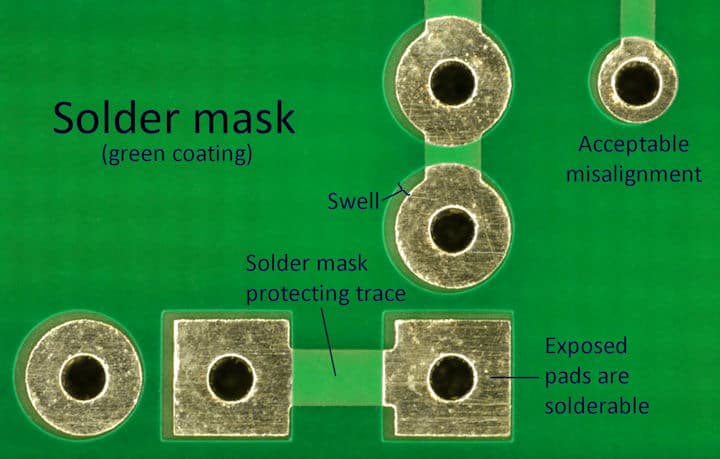
Before discussing the key factors, let's first understand the definition and purpose of solder mask opening. solder mask opening is achieved by applying solder mask material to the pad area and removing specific regions. This helps protect the pads from unintended soldering and short circuits. solder mask opening also helps reduce electromagnetic interference between the pads and other circuit components, thus improving the overall reliability of the circuit.
Next, let's look at the five key factors and best practices for maximizing the effectiveness of solder mask opening on a PCB.
Key Factor 1: Accurate Design of solder mask opening
In the PCB manufacturing process, accurate design of solder mask opening is a crucial factor in achieving optimal solder mask coverage on the pads. A precise design ensures that the solder mask material covers the pads appropriately, while avoiding conflicts with other circuit components and traces. The following aspects will be discussed in detail to ensure accurate design of solder mask opening.
Solder Pad Dimension and Shape:
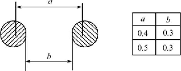
Firstly, determine the dimension and shape of the solder pads based on specific PCB design requirements and application needs. These parameters should consider the functionality of the solder pads, current-carrying capacity, and spacing requirements with other components. Ensuring the reasonable design of solder pad dimension and shape will provide accurate reference for subsequent solder mask opening.
Edge Extension of Solder Mask Material:
To ensure complete protection of the solder pad, the edge of the solder mask material should extend appropriately beyond the boundary of the solder pad. It is recommended to set the extension length of the solder mask material to half the diameter of the solder pad. This ensures sufficient protection of the surrounding area of the solder pad, preventing any unintended short circuits during the soldering process.
Spacing with other components:
When designing solder mask opening, it is important to consider the spacing with other components such as resistors, capacitors, and chips. This is to prevent any conflicts between the solder mask material and other components and to ensure that the quality and connectivity of the solder pads are not affected during the solder mask opening process.
It is essential to plan the spacing between components appropriately, ensuring that there is sufficient space between the solder mask opening area and other components.
Routing and Signal Integrity:
When designing solder mask opening, it is important to consider that the routing areas do not have a negative impact on signal transmission and circuit functionality. Particularly for high-frequency or sensitive signal pads, maintaining good signal integrity is crucial.
When designing solder mask opening, care should be taken to avoid the solder mask material being too close to signal traces or high-frequency components to minimize signal crosstalk and loss.
Application of PCB Design Tools:
In order to achieve precise solder mask opening designs, the use of professional PCB design tools is necessary. These tools provide a wealth of features and options to accurately define the dimensions, shape, and solder mask opening areas of solder pads. By utilizing these tools, designers can ensure consistency and accuracy in their designs, thereby improving the effectiveness and quality of solder mask opening.
Accurate design of solder mask opening is one of the key factors in achieving optimal solder mask opening effects. During the design process, factors such as pad size and shape, edge extension of the solder mask material, spacing with other components, routing, signal integrity, and the use of professional PCB design tools should be considered.
By considering these factors comprehensively, designers can ensure the accuracy and consistency of the solder mask opening areas, thereby achieving the best solder mask opening effects. This will help improve the reliability, performance, and production efficiency of the PCB.
Key Factor 2: Choosing Suitable Solder Mask Material
Choosing suitable solder mask material is one of the key factors to ensure optimal solder mask opening effects. Different solder mask materials have different characteristics and applicability, so it is necessary to select the appropriate material based on specific application requirements.
Polyimide (PI) solder mask material:
Polyimide is a commonly used solder mask material that possesses excellent high-temperature resistance and electrical insulation properties. Due to its outstanding chemical resistance and mechanical strength, PI solder mask material is typically employed in high-reliability applications, such as PCBs in the aerospace sectors.
Additionally, PI solder mask material exhibits low water absorption and excellent dimensional stability, allowing for reliable solder mask protection in complex environmental conditions.
Photosensitive solder mask (PSR) material:
Photosensitive solder mask material is a suitable choice for rapid production and high-density PCBs. PSR material cures under ultraviolet (UV) exposure and exhibits good adhesion and heat resistance. It can provide a thinner solder mask layer, which helps reduce pad size and increase pad density. Additionally, PSR material has low residue and high chemical stability, making it suitable for various application scenarios.
Thermosetting Solder Mask (TSM) Material:
Thermosetting solder mask material is a common choice for solder mask applications, offering excellent high-temperature resistance and chemical stability. TSM materials cure at elevated temperatures to form a hard and wear-resistant solder mask layer. They have high peel strength and mechanical integrity, effectively protecting the solder pads from external environmental and physical damage. TSM materials are typically used in industrial electronics and communication equipment, providing reliable solder pad protection and durability.
When choosing suitable solder mask materials, other factors need to be considered, such as cost, production processes, and environmental requirements. Different materials may have different prices and processing requirements, so it is necessary to weigh various factors to make the best choice. In addition, the compatibility between the solder mask material and other PCB components should also be taken into account to ensure overall performance and reliability.
Choosing the appropriate solder mask material is one of the key factors to ensure the effectiveness of solder mask opening. Evaluating different material options based on application needs and specific requirements, while considering cost, performance, and production requirements, is essential to ensure the best solder mask effectiveness and reliability.
Key Factor 3: Performing Appropriate Surface Treatment for Solder Pads
Surface treatment of solder pads is one of the key factors ensuring the effectiveness of solder mask opening. It directly influences the adhesion and stability of solder mask materials, thus affecting the overall quality and reliability of the solder pads.
When selecting appropriate surface treatment methods for solder pads, factors such as solder pad material, process requirements, and cost-effectiveness need to be considered. The following are detailed descriptions of several common surface treatment methods for solder pads.
Selection of Solder Mask Materials
Before performing surface treatment on solder pads, it is necessary to select appropriate solder mask materials. Common solder mask materials include Polyimide (PI), Photosensitive Solder Resist (PSR), and Thermosetting Solder Resist (TSR). Different materials have distinct characteristics and suitable applications.
For instance, Polyimide exhibits excellent high-temperature resistance and is suitable for soldering applications in high-temperature environments. Photosensitive solder mask materials are suitable for solder mask opening requiring high precision patterns. On the other hand, thermosetting solder mask materials offer higher mechanical strength and chemical resistance. Choosing the appropriate solder mask material based on specific requirements is the first step in ensuring successful surface treatment of solder pads.
Surface Treatment Methods
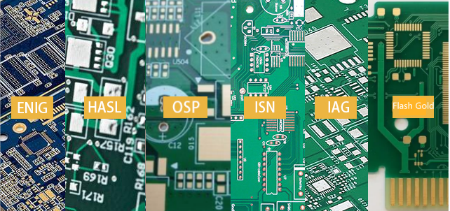
HASL (Hot Air Solder Leveling) is a common surface treatment method for solder pads. It involves immersing the pads into molten solder and then using airflow to blow away the excess solder, resulting in a flat solder pad surface. HASL is a cost-effective method suitable for mass production. However, since the solder leaves a layer of metal coating on the solder pads, it may have some impact on the dimensions and spacing of the pads.ENIG (Electroless Nickel Immersion Gold) is a commonly used high-performance surface treatment method for solder pads. It involves the deposition of a layer of chemical nickel on the surface of the solder pads, followed by a layer of gold on top of the chemical nickel.
This surface treatment method provides excellent flatness, corrosion resistance, and reliability, making it suitable for applications with high soldering process requirements. However, the ENIG method is expensive and is more suitable for small to medium batch production and high-end applications.
OSP (Organic Solderability Preservative) is an environmentally friendly method of surface treatment for solder pads. It involves the formation of an organic protective film on the surface of the solder pads to protect them from oxidation and corrosion.
The OSP method offers advantages such as low cost and stable soldering performance, making it suitable for small to medium batch production and disposable applications. However, solder pads treated with OSP are susceptible to mechanical scratching and chemical corrosion, requiring careful handling and protection during the process.
Surface Treatment Control
Regardless of the chosen method for surface treatment of solder pads, controlling the parameters and conditions of the surface treatment process is crucial to ensure consistency and stability. For example, in the case of the HASL method, it is necessary to control the solder temperature and airflow speed to ensure even distribution of solder and complete blow-off.
In the case of the ENIG method, it is important to control the thickness and uniformity of the electroless nickel and gold coatings. As for the OSP method, it is essential to control the thickness and quality of the protective film. By establishing strict process control and quality inspection systems, the stability and reliability of the solder pad surface treatment can be ensured.
Key Factor 4: Precise Solder Mask Opening Process Control
Precise solder mask opening process control is an essential factor in ensuring the quality and consistency of solder mask opening on the pads. This step involves the control and adjustment of various aspects, such as the uniformity of solder mask material application, accuracy of mask removal, and thermal treatment parameters for the pads.
Firstly, uniform coating is one of the key factors. The solder mask material should be applied evenly and smoothly, matching the size and shape of the solder pads. Uneven coating or defects may result in incomplete or excessive coverage of the solder mask in the solder mask opening area, thereby affecting the quality of the solder joint.
Therefore, it is crucial to ensure the uniform application of the solder mask material by optimizing the coating process, selecting appropriate coating equipment, and adjusting coating parameters.
Furthermore, peel accuracy is also a critical factor. After applying the solder mask material, peeling is necessary to create the opening area. The accuracy of the peeling directly affects the exposed area of the solder pad and the clarity of the boundaries. Oversized or undersized peel areas can both result in poor soldering and be affected.
Therefore, during the peeling process, it is necessary to ensure the accuracy and stability of the peeling tool and follow the correct peeling process parameters to achieve consistent peeling results.
In addition, the thermal treatment parameters of the solder pads also need to be precisely controlled. Thermal treatment involves the preheating and curing processes of the solder pads. The control of preheating temperature and time directly affects the adhesion and stability of the solder mask material, while the control of curing temperature and time affects the degree of hardening and heat resistance of the solder mask material.
Therefore, during the thermal treatment process, it is necessary to accurately set appropriate temperature and time parameters based on the characteristics of the solder mask material and manufacturing requirements and ensure the stability and consistency of the thermal treatment process.
To achieve precise control over the solder mask opening process, advanced equipment and process monitoring techniques are required in the manufacturing process. Automated coating equipment and stripping tools can provide higher accuracy and consistency. Additionally, the use of real-time monitoring and feedback systems can promptly detect and adjust process parameters to ensure that the solder mask opening quality for each pad meets the requirements.
In conclusion, precise control of the solder mask opening process is one of the key factors in achieving optimal solder mask effectiveness. By optimizing coating uniformity, controlling stripping accuracy, and accurately setting thermal processing parameters, the quality, stability, and consistency of solder mask opening can be ensured. This will provide higher reliability and performance in the soldering process during PCB manufacturing, thereby improving the overall product quality.
Key Factor 5: Quality Inspection and Control
Quality inspection and control play a crucial role in maximizing the effectiveness of solder mask opening on PCBs. By conducting rigorous inspection and control of solder mask opening, the stability and consistency of product quality can be ensured. The following are some commonly used methods for quality inspection and control, which will be described in detail.
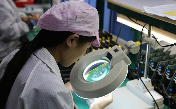
Visual Inspection: Visual inspection is one of the most common and simplest methods of inspection. It involves visually observing the coverage of solder mask opening on the pads to check for any defects, delamination, or areas with incomplete coverage. Workers can use a magnifying glass or microscope for a more detailed examination. This method allows for the quick detection of obvious issues but may not be able to detect small defects.
X-ray Inspection: X-ray inspection can provide more detailed and accurate information on solder mask opening. By using X-ray equipment, the lamination status, coating thickness, and peeling condition of solder mask opening can be observed. This non-destructive testing method can detect small defects and inconsistencies and provides high-resolution images for analysis and evaluation.
Peel Strength Testing: Peel strength testing is one of the key indicators for evaluating the quality of solder mask opening.
This testing method applies force to measure the adhesion strength between the solder mask material and the pads. A dedicated testing apparatus is used to gradually apply force to the pads, and the magnitude of force required to peel off the solder mask material is recorded. Higher peel strength indicates good adhesion between the solder mask material and the pads, ensuring stable quality.
In addition to these specific inspection methods, it is also necessary to establish a comprehensive quality control system to ensure the consistency and stability of solder mask opening. This includes developing clear process specifications and standards, training personnel to ensure operational consistency, and establishing a traceable record and documentation system.
During the quality control process, it is also necessary to collect and analyze data in a timely manner, monitoring key metrics and trends during the production process. Through statistical analysis and data mining techniques, potential issues and improvement opportunities can be identified, and corresponding corrective measures can be implemented.
In addition, maintaining close communication and collaboration with suppliers and partners is also an important aspect of quality control. Establishing strong collaborative relationships ensures that quality standards and requirements are met at every stage of the supply chain, ensuring product consistency and reliability.
Maximizing the solder mask opening effect on PCB pads is an important factor in ensuring the reliability of the circuit board. By designing precise areas for solder mask opening, selecting suitable solder mask materials, performing appropriate surface treatment on the pads, implementing precise process control, and conducting rigorous quality inspection and control, we can ensure the quality and stability of solder mask opening.
Taking these key factors and best practices into consideration during the PCB manufacturing process can enhance product performance, reliability, and production efficiency, thereby meeting various application requirements.
Experience Top-Notch PCB Support with
SprintPCBCount on SprintPCB, the leading high-tech enterprise, for all your PCB manufacturing needs. Our one-stop services cater to clients worldwide, ensuring a hassle-free process at competitive prices. Streamline your operations and reach out to us now to explore the myriad ways in which we can support your organization.